Difference between revisions of "User:Pau pajuelo"
From IGEP - ISEE Wiki
m (→Overview) |
m (→How to use TFT and Touchscreen) |
||
| Line 95: | Line 95: | ||
= What can I do<br> = | = What can I do<br> = | ||
| − | == How to use | + | == How to use HDMI == |
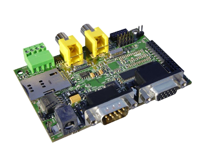
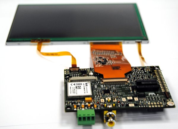
[[Image:IGEP0022 PROTO RA DSC 0142.JPG|right|200px]] IGEPv2 Expansion supports SEIKO 7” or POWERTIP 4.3” LCD screen. Use J301 connector for POWERTRIP 4.3" or use J302, J303 and J304 connector for SEIKO 7".<br> | [[Image:IGEP0022 PROTO RA DSC 0142.JPG|right|200px]] IGEPv2 Expansion supports SEIKO 7” or POWERTIP 4.3” LCD screen. Use J301 connector for POWERTRIP 4.3" or use J302, J303 and J304 connector for SEIKO 7".<br> | ||
Seiko and Powertip touch screens are not supported by default in IGEPv2. Use the following steps for it: | Seiko and Powertip touch screens are not supported by default in IGEPv2. Use the following steps for it: | ||
Revision as of 11:03, 16 October 2013
TODO:
Categorize new tutorials
How to manage the kernel modules on Linux
How do I edit my kernel command line
Basic Software instructions
Make a flash backup to a microSD and restore
Change your static IP to IGEP Firmware
Getting started with IGEP AQUILA EXPANSION
|
|
Overview
This is the 1/3 chapter of IGEP AQUILA Expansion Tutorial Guide.
In this first chapter, we will learn how to connect some expansion peripherals.
Contents
Requirements
In this tutorial we are going to use the following peripherals:
- IGEP AQUILA Expansion with its power supply
- IGEP AQUILA
- Monitor compatible with HDMI
- HDMI cable
- Network cable
- PC
Getting started
Connect IGEPv2 Expansion with IGEPv2 Board
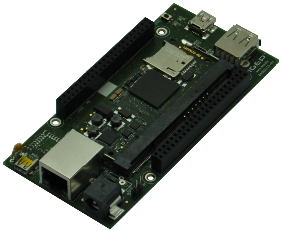
The IGEP AQUILA Expansion connects to the IGEP COM AQUILA Board through K1 and J800 connectors. IGEP AQUILA Expansion should mount J101 jumper to boot from microSD card.
 |
Remote connection via Ethernet

|
If you aren't using a Linux operating system, use IGEP SDK Virtual Machine to connect to the board |
In your Host Machine, open a terminal sessions set up an Ethernet alias for your network interface,
$ sudo ifconfig eth0:0 192.168.5.10
connect to the board using the SSH protocol
$ ssh root@192.168.5.1
an empty password for root user should work to access to the shell prompt.
You have successfully completed this chapter of the guide.
|

|
If you have any question, don't ask to ask at the IGEP Community Forum or the IGEP Community Chat | 
|
|
|
Overview
This is the 2/3 chapter of IGEP AQUILA Expansion Tutorial Guide.
We will learn some basic tasks.
What can I do
How to use HDMI
IGEPv2 Expansion supports SEIKO 7” or POWERTIP 4.3” LCD screen. Use J301 connector for POWERTRIP 4.3" or use J302, J303 and J304 connector for SEIKO 7".Seiko and Powertip touch screens are not supported by default in IGEPv2. Use the following steps for it:
Edit igep.ini file to configure your touch screen, you can do this adding following kernel cmdline parameter
- In Seiko screen add the following line:
omapdss.def_disp=lcd-70
- In Powertip screen add the following line:
omapdss.def_disp=lcd-43
How to use serial console
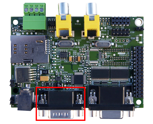
IGEPv2 Expansion integrates a DB9 RS232 connector. This UART is shared with RS485 so it's incompatible use both interfaces at the same time. For that reason to use UART1 for RS232 comunications you should disable RS485 interface. You can do this adding following kernel cmdline parameter.board.ei485=no
You need a Null-Modem DB9 male-make serial cable. Connect the cable between the target board and your PC.
Open the serial port on your PC using your preferred serial communications program (minicom) and configure the port as follows:
- 115200
- 8N1
- no flow control (either software or hardware)
On the target board open a serial port as follows:
$ microcom -s 115200 /dev/ttyS0
Now when you write a character in you PC serial port, the character should appear in the target board.
A detailed guide on how use UARTS can be found by following this link: How to use UARTs
How to use Telit Modem
|
|
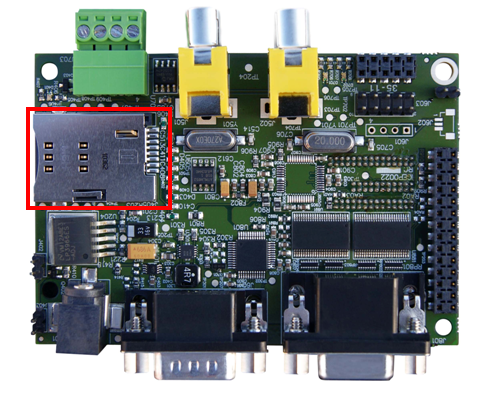
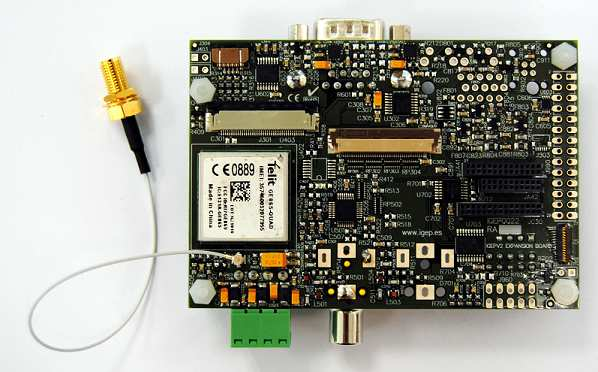
| GSM-GPRS antenna (highly recommended) | SIM card reader |
IGEPv2 Expansion integrates a GSM/GPRS modem to make phone calls or to send SMS or to write and read data from it, etc. Telit modem is not supported by default in IGEPv2 Expansion. Configure this adding following kernel cmdline parameter
buddy.modem=yes
- Power up the modem using the next commands:
$ echo 0 > /sys/class/gpio/gpio140/value
$ echo 1 > /sys/class/gpio/gpio141/value
$ sleep 1
$ echo 0 > /sys/class/gpio/gpio141/value
- Once the modem is on (led near power button is blinking now), you can interact with it via UART 2.
You can use Microcom to comunicate with it from the serial debug console:
$ microcom -s 115200 /dev/ttyO1
- To check the modem status use the command:
at
- Answer should be OK.
- Now unlock it by inserting your SIM card PIN number. Use the command:
at+cpin=<PIN>
- If you correctly inserted the PIN number, the answer should be OK. If you fail more than 3 times, your SIM card will lock and you will have to insert PUK number.
- Now you are ready to use the GSM/GPS modem.
How to use TVP5151 Video Decoder
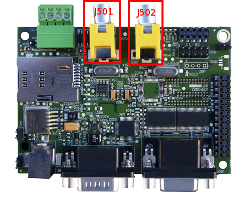
IGEPv2 Expansion integrates two composite video connectors to decode analog input signal.Configure TVP5151
- Plug some peripheral with video composite output in J501 RCA connector, see the image for more details.
- Connect a screen, for example HDMI monitor.
- Refresh repositories and accept it.
$ zypper ref
- Install video4linux2 plugin
$ zypper in gst-plugins-good-video4linux2
Play with TVP5151
- Load OMAP ISP kernel module
$ modprobe omap3-isp
- Configure ISP, for PAL resulution use 720x576 for NTSC resolution use 720x480:
$ media-ctl -r -l '"tvp5150 2-005c":0->"OMAP3 ISP CCDC":0[1], "OMAP3 ISP CCDC":1->"OMAP3 ISP CCDC output":0[1]'
$ media-ctl -v --set-format '"tvp5150 2-005c":0 [UYVY 720x480]'
$ media-ctl -v --set-format '"OMAP3 ISP CCDC":0 [UYVY 720x480]'
$ media-ctl -v --set-format '"OMAP3 ISP CCDC":1 [UYVY 720x480]'
- Export display
$ export DISPLAY=:0.0
- Launch gstreamer
$ gst-launch-0.10 -v v4l2src device=/dev/video2 queue-size=8 ! video/x-raw-yuv,format=\(fourcc\)UYVY,width=720,height=480 ! ffmpegcolorspace ! autovideosink
- Now you can see in your IGEP screen a result similar like this
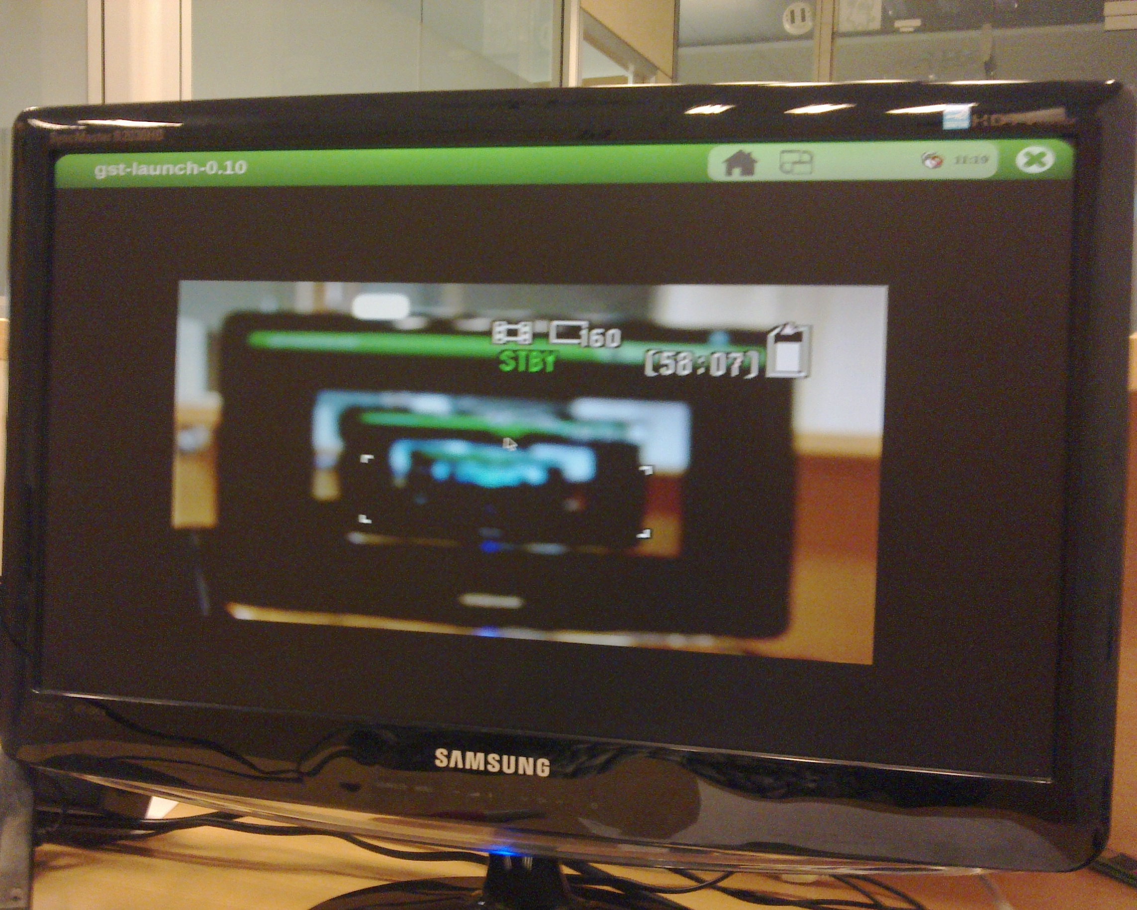
|
From How to setup tvp5151 video decoder
How to use EEPROM
IGEPv2 Expansion includes a serial EEPROM, provides 1KB of user data storage. EEPROM is connected through I2C2 of OMAP3 processor at address 0x50.
The following example writes the value 0x22 to register 0x10 of device 0x50 on i2c bus 2:
$ i2cset -f -y 2 0x50 0x10 0x22
$ i2cget -f -y 2 0x50 0x10
From How to use EEPROM
How to use CAN bus
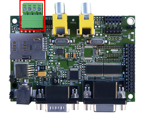
IGEPv2 Expansion integrates a CAN peripheral. Connect any CAN bus device or network to the CAN bus connector (J703).You have to connect the two boards like this:
IGEPv2 Exp 1         IGEPv2 Exp 2
.---                 .---
| 1 |-X            X-| 1 |  VDD_CAN: Supply Voltage (+5V DC)
| 2 |------------------| 2 |  CANL: CAN Low-Level Voltage I/O
| 3 |------------------| 3 |  GND : Ground
| 4 |------------------| 4 |  CANH : CAN High-Level Voltage I/O
.---                 .---
If this is your first time accessing CAN bus, check J702 jumper is not connected before follow this tutorial. If you don't have this jumper, don't worry because its function is only for testing.
Now you can set up the interface (on all boards when using multiple IGEPv2 EXPANSION connected to a CAN network simultaneously):
$ ip link set can0 up type can bitrate 125000
If you want to receive CAN data, use:
$ candump can0
If you want to send CAN data, use:
$ cansend can0 -i 0x123 0xaa 0xbb 0xcc 0xdd
On the receiver side, you must see the following messages:
can0 123 [4] aa bb cc dd
Switch roles and try it again.
From How to use CAN bus
How to use VGA connector
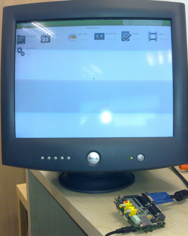
|
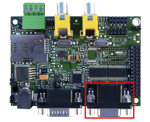
|
IGEPv2 Expansion integrates a VGA connector, the output VGA signal is equal to HDMI connector. Plug a monitor with VGA input.
You have successfully completed this chapter of the guide.
|

|
If you have any question, don't ask to ask at the IGEP Community Forum or the IGEP Community Chat | 
|
IGEP0033 CONNECTOR SUMMARY TABLE
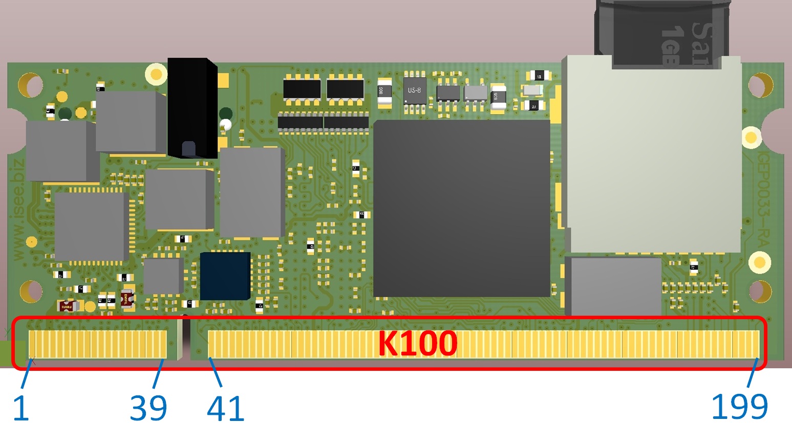
|
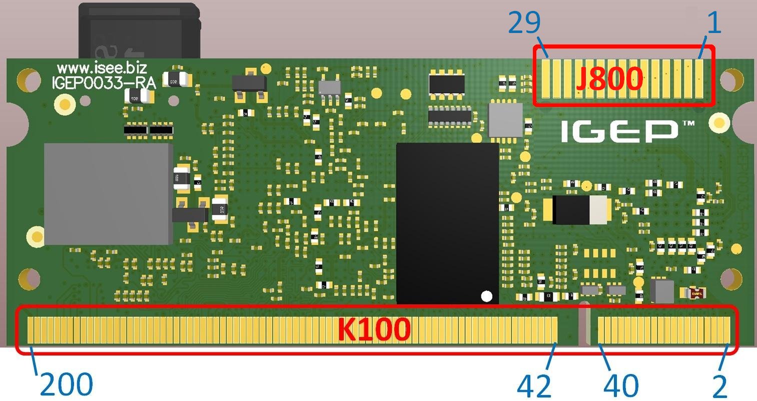
|
| SODIMM-200
|
INTERNAL DEVICE
|
COMMENTS
| ||||||||||
| Pin
|
Type
|
Module Function
|
Dev Pin
|
MODE 0
|
MUX
|
Other MUX
|
GPIO
|
Shared
|
| |||
| 5V INPUT POWER
| ||||||||||||
| 1
|
5V
|
VIN
|
|
PMIC VCCx
|
|
|
|
2,3,4
|
4 pins are used to power the module: 1, 2, 3 and 4 PMIC is the main voltage regulator that generates all the necessary internal voltages. TEXAS INSTRUMENTS P/N: TPS65910A3A1RSL
| |||
| 2
|
5V
|
VIN
|
|
PMIC VCCx
|
|
|
|
1,3,4
| ||||
| 3
|
5V
|
VIN
|
|
PMIC VCCx
|
|
|
|
1,2,4
| ||||
| 4
|
5V
|
VIN
|
|
PMIC VCCx
|
|
|
|
1,2,3
| ||||
| 3V3 OUTPUT POWER
| ||||||||||||
| 5
|
3V3
|
VOUT
|
|
PMIC2 VOUT
|
|
|
|
6,7,9,10,11,12
|
7 pins are used to output 3V3 voltage / 1A for a base board 5,6,7,9,10,11,12
| |||
| 6
|
3V3
|
VOUT
|
|
PMIC2 VOUT
|
|
|
|
5,6,9,10,11,12
| ||||
| 7
|
3V3
|
VOUT
|
|
PMIC2 VOUT
|
|
|
|
5,6,9,10,11,12
| ||||
| BOOT MODE
| ||||||||||||
| 8
|
IN
|
BOOTMODE
|
T1
|
#LCD_DATA4
|
|
GPMC_A4
|
GPIO2_10
|
141
|
BOOT mode select H: from NAND / L: from UART/USB
| |||
| 3V3 OUTPUT POWER
| ||||||||||||
| 9
|
3V3
|
VOUT
|
|
PMIC2 VOUT
|
|
|
|
5,6,7,10,11,12
|
PMIC2 is a linear regulator that supply 3V3 / 1A TEXAS INSTRUMENTS P/N: TPS73701
| |||
| 10
|
3V3
|
VOUT
|
|
PMIC2 VOUT
|
|
|
|
5,6,7,9,11,12
| ||||
| 11
|
3V3
|
VOUT
|
|
PMIC2 VOUT
|
|
|
|
5,6,7,9,10,12
| ||||
| 12
|
3V3
|
VOUT
|
|
PMIC2 VOUT
|
|
|
|
5,6,7,9,10,11
| ||||
| CONTROL SIGNALS
| ||||||||||||
| 13
|
VK
|
VBACKUP
|
27
|
PMIC VBACKUP
|
|
|
|
|
RTC backup power supply. Connect to a 3V1 coin cell battery
| |||
| 14
|
IN
|
PMIC_PWR_BTN
|
33
|
PMIC PWRON
|
|
|
|
|
Power ON Button. Drive to Low to turn off power supply. Refer to PMIC Manual
| |||
| 15
|
OUT
|
#RESET_OUT
|
B14
|
EMU1
|
|
-
|
GPIO3_8
|
|
Active Low Reset Out. Connected to the onboard LAN8720-pin15
| |||
| 16
|
IN
|
#POR
|
B15
|
PWRONRSTn
|
|
-
|
-
|
|
Power ON Reset. Active Low
| |||
| 17
|
IO
|
#RESET_IN
|
A10
|
WARMRSTn
|
|
-
|
-
|
|
Warm Reset. Refer to AM335x Technical Reference Manual
| |||
| 18
|
GND
|
GND
|
|
|
|
|
|
|
Power Ground
| |||
| ETHERNET
| ||||||||||||
| 19
|
ETH
|
ETN_TXN
|
20
|
LAN8720 TXN
|
|
|
|
|
Analog Transmit Data Negative. Differential output to magnetics
| |||
| 20
|
OUT
|
#ETN_LED2
|
2
|
LAN8720 #LED2
|
|
|
|
|
Active Low. LED2 Yellow means 100Mbps speed. Inactive if 10Mbps or line isolation
| |||
| 21
|
ETH
|
ETN_TXP
|
21
|
LAN8720 TXP
|
|
|
|
|
Analog Transmit Data Positive. Differential output to magnetics
| |||
| 22
|
3V3
|
ETN_3V3
|
4
|
PMIC VAUX33
|
|
|
|
|
3V3 to magnetics
| |||
| 23
|
ETH
|
ETN_RXN
|
22
|
LAN8720 RXN
|
|
|
|
|
Analog Receive Data Negative. Differential output to magnetics
| |||
| 24
|
OUT
|
#ETN_LED1
|
3
|
LAN8720 #LED1
|
|
|
|
|
Active Low. LED1 Green indicates valid link and blinks when there is activity
| |||
| 25
|
ETH
|
ETN_RXP
|
23
|
LAN8720 RXP
|
|
|
|
|
Analog Receive Data Poitive. Differential output to magnetics
| |||
| 26
|
GND
|
GND
|
|
|
|
|
|
|
Power Ground
| |||
| USB HOST
| ||||||||||||
| 27
|
OUT
|
USBH_VBUSEN
|
F15
|
USB1_DRVVBUS
|
|
-
|
GPIO3_13
|
|
Active High. Enables external VBUS power supply
| |||
| 28
|
IN
|
#USBH_OC
|
F16
|
USB0_DRVVBUS
|
|
-
|
GPIO0_18
|
|
Active Low. Over current indication to module
| |||
| 29
|
USB
|
USBH_DM
|
R18
|
USB1_DM
|
|
-
|
-
|
|
Analog D- data pin of the USB cable
| |||
| 30
|
USB
|
USBH_VBUS
|
T18
|
USB1_VBUS
|
|
-
|
-
|
|
VBUS pin of the USB cable. Used for the VBUS comparator inputs
| |||
| 31
|
USB
|
USBH_DP
|
R17
|
USB1_DP
|
|
-
|
-
|
|
Analog D+ data pin of the USB cable
| |||
| 32
|
GND
|
GND
|
|
|
|
|
|
|
Power Ground
| |||
| | ||||||||||||
| | ||||||||||||
K100 SODIMM 200 connector
|
SODIMM-200 |
INTERNAL DEVICE |
COMMENTS | ||||||||||
|
Pin |
Type |
Module Function |
Dev Pin |
MODE 0 |
MUX |
Other MUX |
GPIO |
Shared |
||||
|
5V INPUT POWER | ||||||||||||
|
1 |
5V |
VIN |
PMIC VCCx |
2,3,4 |
4 pins are used to power the module: 1, 2, 3 and 4 PMIC is the main voltage regulator that generates all the necessary internal voltages. TEXAS INSTRUMENTS P/N: TPS65910A3A1RSL | |||||||
|
2 |
5V |
VIN |
PMIC VCCx |
1,3,4 | ||||||||
|
3 |
5V |
VIN |
PMIC VCCx |
1,2,4 | ||||||||
|
4 |
5V |
VIN |
PMIC VCCx |
1,2,3 | ||||||||
|
3V3 OUTPUT POWER | ||||||||||||
|
5 |
3V3 |
VOUT |
PMIC2 VOUT |
6,7,9,10,11,12 |
7 pins are used to output 3V3 voltage / 1A for a base board 5,6,7,9,10,11,12 | |||||||
|
6 |
3V3 |
VOUT |
PMIC2 VOUT |
5,6,9,10,11,12 | ||||||||
|
7 |
3V3 |
VOUT |
PMIC2 VOUT |
5,6,9,10,11,12 | ||||||||
|
BOOT MODE | ||||||||||||
|
8 |
IN |
BOOTMODE |
T1 |
#LCD_DATA4 |
GPMC_A4 |
GPIO2_10 |
141 |
BOOT mode select H: from NAND / L: from UART/USB | ||||
|
3V3 OUTPUT POWER | ||||||||||||
|
9 |
3V3 |
VOUT |
PMIC2 VOUT |
5,6,7,10,11,12 |
PMIC2 is a linear regulator that supply 3V3 / 1A TEXAS INSTRUMENTS P/N: TPS73701 | |||||||
|
10 |
3V3 |
VOUT |
PMIC2 VOUT |
5,6,7,9,11,12 | ||||||||
|
11 |
3V3 |
VOUT |
PMIC2 VOUT |
5,6,7,9,10,12 | ||||||||
|
12 |
3V3 |
VOUT |
PMIC2 VOUT |
5,6,7,9,10,11 | ||||||||
|
CONTROL SIGNALS | ||||||||||||
|
13 |
VK |
VBACKUP |
27 |
PMIC VBACKUP |
RTC backup power supply. Connect to a 3V1 coin cell battery | |||||||
|
14 |
IN |
PMIC_PWR_BTN |
33 |
PMIC PWRON |
Power ON Button. Drive to Low to turn off power supply. Refer to PMIC Manual | |||||||
|
15 |
OUT |
#RESET_OUT |
B14 |
EMU1 |
- |
GPIO3_8 |
Active Low Reset Out. Connected to the onboard LAN8720-pin15 | |||||
|
16 |
IN |
#POR |
B15 |
PWRONRSTn |
- |
- |
Power ON Reset. Active Low | |||||
|
17 |
IO |
#RESET_IN |
A10 |
WARMRSTn |
- |
- |
Warm Reset. Refer to AM335x Technical Reference Manual | |||||
|
18 |
GND |
GND |
Power Ground | |||||||||
|
ETHERNET | ||||||||||||
|
19 |
ETH |
ETN_TXN |
20 |
LAN8720 TXN |
Analog Transmit Data Negative. Differential output to magnetics | |||||||
|
20 |
OUT |
#ETN_LED2 |
2 |
LAN8720 #LED2 |
Active Low. LED2 Yellow means 100Mbps speed. Inactive if 10Mbps or line isolation | |||||||
|
21 |
ETH |
ETN_TXP |
21 |
LAN8720 TXP |
Analog Transmit Data Positive. Differential output to magnetics | |||||||
|
22 |
3V3 |
ETN_3V3 |
4 |
PMIC VAUX33 |
3V3 to magnetics | |||||||
|
23 |
ETH |
ETN_RXN |
22 |
LAN8720 RXN |
Analog Receive Data Negative. Differential output to magnetics | |||||||
|
24 |
OUT |
#ETN_LED1 |
3 |
LAN8720 #LED1 |
Active Low. LED1 Green indicates valid link and blinks when there is activity | |||||||
|
25 |
ETH |
ETN_RXP |
23 |
LAN8720 RXP |
Analog Receive Data Poitive. Differential output to magnetics | |||||||
|
26 |
GND |
GND |
Power Ground | |||||||||
|
USB HOST | ||||||||||||
|
27 |
OUT |
USBH_VBUSEN |
F15 |
USB1_DRVVBUS |
- |
GPIO3_13 |
Active High. Enables external VBUS power supply | |||||
|
28 |
IN |
#USBH_OC |
F16 |
USB0_DRVVBUS |
- |
GPIO0_18 |
Active Low. Over current indication to module | |||||
|
29 |
USB |
USBH_DM |
R18 |
USB1_DM |
- |
- |
Analog D- data pin of the USB cable | |||||
|
30 |
USB |
USBH_VBUS |
T18 |
USB1_VBUS |
- |
- |
VBUS pin of the USB cable. Used for the VBUS comparator inputs | |||||
|
31 |
USB |
USBH_DP |
R17 |
USB1_DP |
- |
- |
Analog D+ data pin of the USB cable | |||||
|
32 |
GND |
GND |
Power Ground | |||||||||
|
USB OTG | ||||||||||||
|
33 |
USB |
USBOTG_ID |
P16 |
USB0_ID |
- |
- |
ID pin of the USB cable. A-device is grounded; B-device is floating | |||||
|
34 |
OUT |
USBOTG_VBUSEN |
R13 |
GPMC_A0 |
GPIO1_16 |
GPMC_A16 |
GPIO1_16 |
156 |
Active High. Enables external VBUS power supply | |||
|
35 |
USB |
USBOTG_DM |
N18 |
USB0_DM |
- |
- |
Analog D- data pin of the USB cable | |||||
|
36 |
IN |
#USBOTG_OC |
V17 |
GPMC_A11 |
GPIO1_27 |
GPMC_A27 |
GPIO1_27 |
152 |
Active Low. Over current indication to module | |||
|
37 |
USB |
USBOTG_DP |
N17 |
USB0_DP |
- |
- |
Analog D+ data pin of the USB cable | |||||
|
38 |
IN |
USBOTG_VBUS |
P15 |
USB0_VBUS |
- |
- |
VBUS pin of the USB cable. Used for the VBUS comparator inputs | |||||
|
39 |
GND |
GND |
Power Ground | |||||||||
|
I2C INTERFACE | ||||||||||||
|
40 |
IO |
I2C_DATA |
C17 |
I2C0_SDA |
TIMER4 |
GPIO3_5 |
PMIC pin 8 |
I2C bus data. Shared device on this bus and address: PMIC @2D (HEXA) | ||||
|
41 |
IO |
I2C_CLK |
C16 |
I2C0_SCL |
TIMER7 |
GPIO3_6 |
PMIC pin 9 |
I2C bus clock | ||||
|
PWM | ||||||||||||
|
42 |
OUT |
PWM |
A13 |
MCASP0_ACLKX |
EHRPWM0A |
MMC0_SDCD |
GPIO3_14 |
95 & sd_cd |
PWM Output. Shared internally with SD CD. Configured by default as MMC0_SDCD | |||
|
OWIRE: ONE WIRE INTERFACE | ||||||||||||
|
43 |
IO |
OWDAT |
V14 |
GPMC_A1 |
GPIO1_17 |
GPMC_A17 |
GPIO1_17 |
148 |
AM335x has not 1-wire controller. GPIO1_17 is used. Requires pull up. | |||
|
CSPI: SERIAL PERIPHERAL INTERFACE | ||||||||||||
|
44 |
OUT |
CSPI_SS0 |
A16 |
SPI0_CS0 |
I2C1_SCL |
GPIO0_5 |
SPI Slave select signal | |||||
|
45 |
OUT |
CSPI_SS1 |
C15 |
SPI0_CS1 |
UART3_RXD |
GPIO0_6 |
SPI Slave select signal | |||||
|
46 |
OUT |
CSPI_MOSI |
B17 |
SPI0_D0 |
I2C2_SCL |
GPIO0_3 |
SPI Master Output-Slave Input | |||||
|
47 |
IN |
CSPI_MISO |
B16 |
SPI0_D1 |
I2C1_SDA |
GPIO0_4 |
SPI Master Input-Slave Output | |||||
|
48 |
OUT |
CSPI_SCLK |
A17 |
SPI0_SCLK |
I2C2_SDA |
GPIO0_2 |
SPI Clock | |||||
|
49 |
OUT |
CSPI_RDY |
Not connected | |||||||||
|
50 |
GND |
GND |
Power Ground | |||||||||
|
uSD1: SECURE DIGITAL INTERFACE 1 | ||||||||||||
|
51 |
IN |
SD1_CD |
B13 |
MCASP0_FSX |
MMC1_SDCD |
EHRPWM0B |
GPIO3_15 |
SD CARD Detect | ||||
|
52 |
IO |
SD1_D0 |
K18 |
MII1_TX_CLK |
MMC1_DAT0 |
UART2_RXD |
GPIO3_9 |
SD Data 0 bidirectional. User must pull up this signal accordingly | ||||
|
53 |
IO |
SD1_D1 |
L18 |
MII1_RX_CLK |
MMC1_DAT1 |
UART2_TXD |
GPIO3_10 |
SD Data 1 bidirectional. User must pull up this signal accordingly | ||||
|
54 |
IO |
SD1_D2 |
L17 |
MII1_RXD3 |
MMC1_DAT2 |
UART3_RXD |
GPIO2_18 |
SD Data 2 bidirectional. User must pull up this signal accordingly | ||||
|
55 |
IO |
SD1_D3 |
L16 |
MII1_RXD2 |
MMC1_DAT3 |
UART3_TXD |
GPIO2_19 |
SD Data 3 bidirectional. User must pull up this signal accordingly | ||||
|
56 |
IO |
SD1_CMD |
V9 |
GPMC_CSn2 |
MMC1_CMD |
GPMC_BE1N |
GPIO1_31 |
SD command bidirectional data | ||||
|
57 |
IO |
SD1_CLK |
U9 |
GPMC_CSn1 |
MMC1_CLK |
GPMC_CLK |
GPIO1_30 |
SD Output clock | ||||
|
58 |
GND |
GND |
Power Ground | |||||||||
|
1ST UART | ||||||||||||
|
59 |
OUT |
UART1_TXD |
E16 |
UART0_TXD |
SPI1_CS1 |
GPIO1_11 |
Debug UART Transmit Data Output | |||||
|
60 |
IN |
UART1_RXD |
E15 |
UART0_RXD |
SPI1_CS0 |
GPIO1_10 |
Debug UART Receive Data Intput | |||||
|
61 |
IN |
UART1_RTS/CTS IN |
E18 |
UART0_CTSn |
SPI1_D0 |
GPIO1_8 |
Debug UART RTS/CTS INPUT | |||||
|
62 |
OUT |
UART1_CTS/RTS OUT |
E17 |
UART0_RTSn |
SPI1_D1 |
GPIO1_9 |
Debug UART RTS/CTS OUTPUT | |||||
|
2ND UART | ||||||||||||
|
63 |
OUT |
UART2_TXD |
D15 |
UART1_TXD |
DCAN1_RX |
GPIO0_15 |
UART Transmit Data Output | |||||
|
64 |
IN |
UART2_RXD |
D16 |
UART1_RXD |
DCAN1_TX |
GPIO0_14 |
UART Receive Data Intput | |||||
|
65 |
IN |
UART2_RTS/CTS IN |
D18 |
UART1_CTSn |
DCAN0_TX |
GPIO0_12 |
UART RTS/CTS INPUT | |||||
|
66 |
OUT |
UART2_CTS/RTS OUT |
D17 |
UART1_RTSn |
DCAN0_RX |
GPIO0_13 |
UART RTS/CTS OUTPUT | |||||
|
3RD UART | ||||||||||||
|
67 |
OUT |
UART3_TXD |
J17 |
MII1_RX_DV |
UART5_TXD |
MMC2_DAT0 |
GPIO3_4 |
UART Transmit Data Output | ||||
|
68 |
IN |
UART3_RXD |
H16 |
MII1_COL |
UART5_RXD |
SPI1_SCLK |
GPIO3_0 |
UART Receive Data Intput | ||||
|
69 |
IN |
UART3_RTS/CTS IN |
G15 |
MMC0_DAT1 |
UART5_CTSN |
UART3_RXD |
GPIO2_28 |
97 & sd_d1 |
UART RTS/CTS INPUT. Shared with internal SD D1. Configured as MMC0_DAT1 | |||
|
70 |
OUT |
UART3_CTS/RTS OUT |
G16 |
MMC0_DAT0 |
UART5_RTSN |
UART3_TXD |
GPIO2_29 |
96 & sd_d0 |
UART RTS/CTS OUTPUT. Shared with internal SD D0. Configured as MMC0_DAT0 | |||
|
71 |
GND |
GND |
Power Ground | |||||||||
|
KEYPAD / CAN | ||||||||||||
|
72 |
IN |
KP_COL0 |
U16 |
GPMC_A9 |
GPIO1_25 |
GPMC_A25 |
GPIO1_25 |
159 |
KeyPAD Column 0. Pin shared with SODIMM pin 159 | |||
|
73 |
IN |
KP_COL1 |
C12 |
MCASP0_AHCLKR |
GPIO3_17 |
EHRPWM0_SYNCI |
GPIO3_17 |
KeyPAD Column 1 | ||||
|
74 |
IN |
KP_COL2 |
C18 |
ECAP0_IN_PWM0_OUT |
GPIO0_7 |
UART3_TXD |
GPIO0_7 |
KeyPAD Column 2 | ||||
|
75 |
IN |
KP_COL3 |
U18 |
GPMC_BEn1 |
GPIO1_28 |
GPMC_DIR |
GPIO1_28 |
KeyPAD Column 3 | ||||
|
76 |
OUT |
TXCAN |
J18 |
MII1_TXD3 |
DCAN0_TX |
UART4_RXD |
GPIO0_16 |
CAN Transmission line | ||||
|
77 |
IN |
KP_ROW0 |
A15 |
XDMA_EVENT_INTR0 |
GPIO0_19 |
TIMER4 |
GPIO0_19 |
KeyPAD Row 0 | ||||
|
78 |
IN |
KP_ROW1 |
D14 |
XDMA_EVENT_INTR1 |
GPIO0_20 |
TIMER7 |
GPIO0_20 |
KeyPAD Row 1 | ||||
|
79 |
IN |
KP_ROW2 |
V12 |
GPMC_CLK |
GPIO2_1 |
MMC2_CLK |
GPIO2_1 |
KeyPAD Row 2 | ||||
|
80 |
IN |
KP_ROW3 |
T13 |
GPMC_CSn3 |
GPIO2_0 |
MMC2_CMD |
GPIO2_0 |
KeyPAD Row 3 | ||||
|
81 |
IN |
RXCAN |
K15 |
MII1_TXD2 |
DCAN0_RX |
UART4_TXD |
GPIO0_17 |
CAN Reception line | ||||
|
82 |
GND |
GND |
Power Ground | |||||||||
|
SSI 1: SERIAL AUDIO PORT 1 | ||||||||||||
|
83 |
IO |
SSI1_INT |
D12 |
MCASP0_AXR0 |
GPIO3_16 |
MMC2_SDCD |
GPIO3_16 |
Serial Audio Interface Interrupt signal | ||||
|
84 |
IO |
SSI1_RXD |
D13 |
MCASP0_AXR1 |
MCASP1_AXR0 |
EMU3 |
GPIO3_20 |
Serial Audio Interface serial data line 0 | ||||
|
85 |
IO |
SSI1_TXD |
A14 |
MCASP0_AHCLKX |
MCASP1_AXR1 |
EMU4 |
GPIO3_21 |
Serial Audio Interface serial data line 1 | ||||
|
86 |
IO |
SSI1_CLK |
B12 |
MCASP0_ACLKR |
MCASP1_ACLKX |
MMC0_SDWP |
GPIO3_18 |
Serial Audio Interface serial clock | ||||
|
87 |
IO |
SSI1_FS |
C13 |
MCASP0_FSR |
MCASP1_FSX |
EMU2 |
GPIO3_19 |
Serial Audio Interface left/right clock | ||||
|
88 |
GND |
GND |
Power Ground | |||||||||
|
SSI 2: SERIAL AUDIO PORT 2 | ||||||||||||
|
89 |
SSI2_INT |
Not connected | ||||||||||
|
90 |
SSI2_RXD |
Not connected | ||||||||||
|
91 |
SSI2_TXD |
Not connected | ||||||||||
|
92 |
SSI2_CLK |
Not connected | ||||||||||
|
93 |
SSI2_FS |
Not connected | ||||||||||
|
94 |
GND |
GND |
Power Ground | |||||||||
|
uSD2: SECURE DIGITAL INTERFACE 2 | ||||||||||||
|
95 |
IN |
SD2_CD |
A13 |
MCASP0_ACLKX |
MMC0_SDCD |
EHRPWM0A |
GPIO3_14 |
42 & sd_cd |
SD Card detect. Shared internally with SD CD. It can be configured as PWM output | |||
|
96 |
IO |
SD2_D0 |
G16 |
MMC0_DAT0 |
UART5_RTSN |
GPIO2_29 |
70 & sd_d0 |
SD Data 1 bidirectional. Shared internally with SD D0. It can be configured as UART_RTSN | ||||
|
97 |
IO |
SD2_D1 |
G15 |
MMC0_DAT1 |
UART5_CTSN |
GPIO2_28 |
69 & sd_d1 |
SD Data 1 bidirectional. Shared internally with SD D1. It can be configured as UART_CTSN | ||||
|
98 |
IO |
SD2_D2 |
F18 |
MMC0_DAT2 |
TIMER6 |
GPIO2_27 |
sd_d2 |
SD Data 2 bidirectional. Shared internally with SD D2 | ||||
|
99 |
IO |
SD2_D3 |
F17 |
MMC0_DAT3 |
TIMER5 |
GPIO2_26 |
sd_d3 |
SD Data 3 bidirectional. Shared internally with SD D3 | ||||
|
100 |
IO |
SD2_CMD |
G18 |
MMC0_CMD |
DCAN1_RX |
GPIO2_31 |
sd_cmd |
SD CMD bidirectional. Shared internally with SD CMD | ||||
|
101 |
SD2_CLK |
G17 |
MMC0_CLK |
DCAN1_TX |
GPIO2_30 |
sd_clk |
SD Clock bidirectional. Shared internally with SD CK | |||||
|
102 |
GND |
GND |
Power Ground | |||||||||
|
CMOS SENSOR INTERFACE | ||||||||||||
|
103 |
CSI_D0 |
Not connected | ||||||||||
|
104 |
CSI_D1 |
Not connected | ||||||||||
|
105 |
CSI_D2 |
Not connected | ||||||||||
|
106 |
CSI_D3 |
Not connected | ||||||||||
|
107 |
CSI_D4 |
Not connected | ||||||||||
|
108 |
CSI_D5 |
Not connected | ||||||||||
|
109 |
CSI_D6 |
Not connected | ||||||||||
|
110 |
CSI_D7 |
Not connected | ||||||||||
|
111 |
GND |
GND |
Power Ground | |||||||||
|
112 |
CSI_HSYNC |
Not connected | ||||||||||
|
113 |
CSI_VSYNC |
Not connected | ||||||||||
|
114 |
CSI_PIXCLK |
Not connected | ||||||||||
|
115 |
CSI_MCLK |
Not connected | ||||||||||
|
116 |
GND |
GND |
Power Ground | |||||||||
|
LCD CONTROLLER | ||||||||||||
|
117 |
OUT |
LCD_D0 |
U10 |
GPMC_AD8 |
LCD_DATA23 |
EHRPWM2A |
GPIO0_22 |
LCD DATA BUS | ||||
|
118 |
OUT |
LCD_D1 |
U12 |
GPMC_AD11 |
LCD_DATA20 |
MMC2_DAT7 |
GPIO0_27 |
LCD DATA BUS | ||||
|
119 |
OUT |
LCD_D2 |
V13 |
GPMC_AD14 |
LCD_DATA17 |
MMC2_DAT2 |
GPIO1_14 |
LCD DATA BUS | ||||
|
120 |
IO |
LCD_D3 |
U4 |
LCD_DATA11 |
GPMC_A15 |
GPIO2_17 |
LCD DATA BUS / SYS_BOOT11 | |||||
|
121 |
IO |
LCD_D4 |
V2 |
LCD_DATA12 |
GPMC_A16 |
GPIO0_8 |
LCD DATA BUS / SYS_BOOT12 | |||||
|
122 |
IO |
LCD_D5 |
V3 |
LCD_DATA13 |
GPMC_A17 |
GPIO0_9 |
LCD DATA BUS / SYS_BOOT13 | |||||
|
123 |
IO |
LCD_D6 |
V4 |
LCD_DATA14 |
GPMC_A18 |
GPIO0_10 |
LCD DATA BUS / SYS_BOOT14 | |||||
|
124 |
IO |
LCD_D7 |
T5 |
LCD_DATA15 |
GPMC_A19 |
GPIO0_11 |
LCD DATA BUS / SYS_BOOT15 | |||||
|
125 |
OUT |
LCD_D8 |
T10 |
GPMC_AD9 |
LCD_DATA22 |
EHRPWM2B |
GPIO0_23 |
LCD DATA BUS | ||||
|
126 |
OUT |
LCD_D9 |
T12 |
GPMC_AD12 |
LCD_DATA19 |
MMC2_DAT0 |
GPIO1_12 |
LCD DATA BUS | ||||
|
127 |
IO |
LCD_D10 |
T2 |
LCD_DATA5 |
GPMC_A5 |
GPIO2_11 |
LCD DATA BUS / SYS_BOOT5 | |||||
|
128 |
OUT |
LCD_D11 |
T3 |
LCD_DATA6 |
GPMC_A6 |
GPIO2_12 |
LCD DATA BUS / SYS_BOOT6 | |||||
|
129 |
GND |
GND |
Power Ground | |||||||||
|
130 |
IO |
LCD_D12 |
T4 |
LCD_DATA7 |
GPMC_A7 |
GPIO2_13 |
LCD DATA BUS / SYS_BOOT7 | |||||
|
131 |
IO |
LCD_D13 |
U1 |
LCD_DATA8 |
GPMC_A12 |
GPIO2_14 |
LCD DATA BUS / SYS_BOOT8 | |||||
|
132 |
IO |
LCD_D14 |
U2 |
LCD_DATA9 |
GPMC_A13 |
GPIO2_15 |
LCD DATA BUS / SYS_BOOT9 | |||||
|
133 |
IO |
LCD_D15 |
U3 |
LCD_DATA10 |
GPMC_A14 |
GPIO2_16 |
LCD DATA BUS / SYS_BOOT10 | |||||
|
134 |
OUT |
LCD_D16 |
T11 |
GPMC_AD10 |
LCD_DATA21 |
MMC2_DAT6 |
GPIO0_26 |
LCD DATA BUS | ||||
|
135 |
OUT |
LCD_D17 |
R12 |
GPMC_AD13 |
LCD_DATA18 |
MMC2_DAT1 |
GPIO1_13 |
LCD DATA BUS | ||||
|
136 |
OUT |
LCD_D18 |
U13 |
GPMC_AD15 |
LCD_DATA16 |
MMC2_DAT3 |
GPIO1_15 |
LCD DATA BUS | ||||
|
137 |
IO |
LCD_D19 |
R1 |
LCD_DATA0 |
GPMC_A0 |
GPIO2_6 |
JTAG7 |
LCD DATA BUS / SYS_BOOT0 | ||||
|
138 |
IO |
LCD_D20 |
R2 |
LCD_DATA1 |
GPMC_A1 |
GPIO2_7 |
JTAG5 |
LCD DATA BUS / SYS_BOOT1 | ||||
|
139 |
IO |
LCD_D21 |
R3 |
LCD_DATA2 |
GPMC_A2 |
GPIO2_8 |
LCD DATA BUS / SYS_BOOT2 | |||||
|
140 |
IO |
LCD_D22 |
R4 |
LCD_DATA3 |
GPMC_A3 |
GPIO2_9 |
LCD DATA BUS / SYS_BOOT3 | |||||
|
141 |
IO |
LCD_D23 |
T1 |
LCD_DATA4 |
GPMC_A4 |
GPIO2_10 |
8 |
LCD DATA BUS / SYS_BOOT4 | ||||
|
142 |
GND |
GND |
Power Ground | |||||||||
|
143 |
OUT |
LCD_HSYNC |
R5 |
LCD_HSYNC |
GPMC_A9 |
GPIO2_23 |
LCD BUS HORIZONTAL SYNCHRONISM | |||||
|
144 |
OUT |
LCD_VSYNC |
U5 |
LCD_VSYNC |
GPMC_A8 |
GPIO2_22 |
LCD BUS VERTICAL SYNCHRONISM | |||||
|
145 |
OUT |
LCD_OE_ACD |
R6 |
LCD_AC_BIAS_EN |
GPMC_A11 |
GPIO2_25 |
LCD BUS CONTROL | |||||
|
146 |
OUT |
LCD_SCLK |
V5 |
LCD_PCLK |
GPMC_A10 |
GPIO2_24 |
LCD BUS CLOCK | |||||
|
147 |
GND |
GND |
Power Ground | |||||||||
|
IGEPTM COM CYGNUS and IGEPTM COM AQUILA MODULES SPECIFIC SIGNALS | ||||||||||||
|
148 |
IO |
GPIO0 |
V14 |
GPMC_A1 |
GPIO1_17 |
GPMC_A17 |
GPIO1_17 |
43 |
I/O SHARED WITH SODIMM pin 43 OWDAT one wire | |||
|
149 |
IO |
GPIO1 |
U14 |
GPMC_A2 |
GPIO1_18 |
GPMC_A18 |
GPIO1_18 |
I/O | ||||
|
150 |
IO |
GPIO2 |
T14 |
GPMC_A3 |
GPIO1_19 |
GPMC_A19 |
GPIO1_19 |
I/O | ||||
|
151 |
IO |
GPIO3 |
U15 |
GPMC_A6 |
GPIO1_22 |
GPMC_A22 |
GPIO1_22 |
I/O | ||||
|
152 |
IO |
GPIO4 |
V17 |
GPMC_A11 |
GPIO1_27 |
GPMC_A27 |
GPIO1_27 |
36 |
I/O SHARED WITH SODIMM pin 36 #USBOTG_OC | |||
|
153 |
IO |
GPIO5 |
T16 |
GPMC_A10 |
GPIO1_26 |
GPMC_A26 |
GPIO1_26 |
I/O | ||||
|
154 |
IO |
GPIO6 |
V15 |
GPMC_A5 |
GPIO1_21 |
GPMC_A21 |
GPIO1_21 |
I/O | ||||
|
155 |
IO |
GPIO7 |
R14 |
GPMC_A4 |
GPIO1_20 |
GPMC_A20 |
GPIO1_20 |
I/O | ||||
|
156 |
IO |
GPIO8 |
R13 |
GPMC_A0 |
GPIO1_16 |
GPMC_A16 |
GPIO1_16 |
34 |
I/O SHARED WITH SODIMM pin 34 USBOTG_VBUSEN | |||
|
157 |
IO |
GPIO9 |
T15 |
GPMC_A7 |
GPIO1_23 |
GPMC_A23 |
GPIO1_23 |
USER LED |
I/O SHARED WITH USER LED | |||
|
158 |
IO |
GPIO10 |
V16 |
GPMC_A8 |
GPIO1_24 |
GPMC_A24 |
GPIO1_24 |
PMIC pin37 |
I/O SHARED WITH REGULATOR SLEEP | |||
|
159 |
IO |
GPIO11 |
U16 |
GPMC_A9 |
GPIO1_25 |
GPMC_A25 |
GPIO1_25 |
72 |
I/O SHARED WITH SODIMM pin 72 KEYCOL0 | |||
|
160 |
GND |
GND |
Power Ground | |||||||||
|
161 |
OUT |
GPMC_WPn |
U17 |
GPMC_WPn |
GPMC_CSN5 |
GPIO0_31 |
NAND |
SHARED WITH NAND FLASH MEMORY WPN | ||||
|
162 |
NC |
Not connected | ||||||||||
|
163 |
NC |
Not connected | ||||||||||
|
164 |
NC |
Not connected | ||||||||||
|
165 |
NC |
Not connected | ||||||||||
|
166 |
NC |
Not connected | ||||||||||
|
167 |
NC |
Not connected | ||||||||||
|
168 |
NC |
Not connected | ||||||||||
|
169 |
NC |
Not connected | ||||||||||
|
170 |
NC |
Not connected | ||||||||||
|
171 |
GND |
GND |
Power Ground | |||||||||
|
172 |
NC |
Not connected | ||||||||||
|
173 |
NC |
Not connected | ||||||||||
|
174 |
NC |
Not connected | ||||||||||
|
175 |
NC |
Not connected | ||||||||||
|
176 |
NC |
Not connected | ||||||||||
|
177 |
NC |
Not connected | ||||||||||
|
178 |
NC |
Not connected | ||||||||||
|
179 |
OUT |
GPMC_BEn0_CLE |
T6 |
GPMC_BEn0_CLE |
TIMER5 |
GPIO2_5 |
NAND |
SHARED WITH NAND FLASH MEMORY | ||||
|
180 |
OUT |
GPMC_ADVn_ALE |
R7 |
GPMC_ADVn_ALE |
TIMER4 |
GPIO2_2 |
NAND |
SHARED WITH NAND FLASH MEMORY | ||||
|
181 |
OUT |
GPMC_WEn |
U6 |
GPMC_WEn |
TIMER6 |
GPIO2_4 |
NAND |
SHARED WITH NAND FLASH MEMORY | ||||
|
182 |
OUT |
GPMC_OEn_REn |
T7 |
GPMC_OEn_REn |
TIMER7 |
GPIO2_3 |
NAND |
SHARED WITH NAND FLASH MEMORY | ||||
|
183 |
GND |
GND_ADC |
E8 |
VSSA_ADC |
Analog Ground | |||||||
|
184 |
NC |
Not connected | ||||||||||
|
185 |
ADC |
XN |
B6 |
AIN0 |
- |
- |
TOUCHSCREEN ADC INPUT CHANNEL | |||||
|
186 |
ADC |
XP |
C7 |
AIN1 |
- |
- |
TOUCHSCREEN ADC INPUT CHANNEL | |||||
|
187 |
ADC |
YN |
B7 |
AIN2 |
- |
- |
TOUCHSCREEN ADC INPUT CHANNEL | |||||
|
188 |
ADC |
YP |
A7 |
AIN3 |
- |
- |
TOUCHSCREEN ADC INPUT CHANNEL | |||||
|
189 |
ADC |
WIPER |
C8 |
AIN4 |
- |
- |
TOUCHSCREEN ADC INPUT CHANNEL | |||||
|
190 |
ADC |
ADC5 |
B8 |
AIN5 |
- |
- |
GENERAL PURPOSE ADC CHANNEL | |||||
|
191 |
ADC |
ADC6 |
A8 |
AIN6 |
- |
- |
GENERAL PURPOSE ADC CHANNEL | |||||
|
192 |
ADC |
ADC7 |
C9 |
AIN7 |
- |
- |
GENERAL PURPOSE ADC CHANNEL | |||||
|
193 |
IN |
WAKEUP |
C5 |
EXT_WAKEUP |
- |
- |
EXTERNAL WAKE UP | |||||
|
194 |
NC |
Not connected | ||||||||||
|
195 |
NC |
Not connected | ||||||||||
|
196 |
NC |
Not connected | ||||||||||
|
197 |
IO |
- |
C14 |
EMU0 |
GPIO3_7 |
- |
GPIO3_7 |
|||||
|
198 |
OUT |
MDC |
M18 |
MDIO_CLK |
TIMER5 |
GPIO0_1 |
LAN8720 pin13 |
SHARED WITH ETHERNET PHY | ||||
|
199 |
IO |
MDIO |
M17 |
MDIO_DATA |
TIMER6 |
GPIO0_0 |
LAN8720 pin12 |
SHARED WITH ETHERNET PHY | ||||
|
200 |
GND |
GND |
Power Ground | |||||||||
OLD introduction
| Pad | Pad name | Main utility | BASE0033 utility | Other available peripherals | Share with |
| 5V INPUT POWER | |||||
| 1 2 3 4 |
VIN | VDD_5V: Input 5V |
VDD_5V: Input 5V |
- | - |
| 3V3 OUTPUT POWER | |||||
| 5 6 7 |
VOUT | VDD_3V3: Output 3V3 |
VDD_3V3: Output 3V3 |
- | - |
| BOOT MODE | |||||
| 8 | BOOTMODE | - | - | ||
| 3V3 OUTPUT POWER | |||||
| 9 10 11 12 |
VOUT | VDD_3V3: Output 3V3 |
VDD_3V3: Output 3V3 |
- | - |
| CONTROL SIGNALS | |||||
| ETHERNET | |||||
| USB HOST | |||||
| USB OTG | |||||
| I2C INTERFACE | |||||
| PWM | |||||
| OWIRE: ONE WIRE INTERFACE | |||||
| CSPI: SERIAL PERIPHERAL INTERFACE | |||||
| uSD1: SECURE DIGITAL INTERFACE 1 | |||||
| 1st UART | |||||
| 2nd UART | |||||
| 3rd UART | |||||
| KEYPAD/CAN | |||||
| SSI 1: SERIAL AUDIO PORT 1 | |||||
| SSI 2: SERIAL AUDIO PORT 2 | |||||
| uSD2: SECURE DIGITAL INTERFACE 2 | |||||
| CMOS SENSOR INTERFACE | |||||
| LCD CONTROLLER | |||||
| MODULE SPECIFIC SIGNALS | |||||
BASE0033 CONNECTOR SUMMARY TABLE
Configure a static IP using the same private network range
under construction
IGEP Firmware Yocto uses the following Ethernet network configuration (IP addresses)
- eth0 − 192.168.5.1
- eth0:0 − assigned via dhcp.
This Ethernet network configuration is really useful when you work using a Linux operating system like IGEP SDK Virtual Machine. Because you use eth0 device to communicate easily with your board and eth0:0 device to get Internet acces using dhcp protocol.
But some scenarios this network configuration is not useful, for example: if you use a non-Linux operating system, connect to two IP private range interfaces is not simple. This How-to can be useful to
(Make diagram one: IGEP and Linux defualt communication. Diagram 2 IGEP and other SO alternative configuration)
igep.ini parameters
The kernel command line syntax is name=value1. These next parameters are supported in igep.ini since IGEP-X_Loader 2.4.0-2:
[kernel]
| Parameter Name | Description | Default value | Comments |
| kaddress | Kernel copy address | =0x80008000 | Hex memory address |
| rdaddress | Ram Disk location address | =0x81600000 | Hex memory address; disabled by default |
| serial.low | Serial number (low part) | =00000001 | Numeric |
| serial.high | Serial number (high part) | =00000000 | Numeric |
| revision | Revision ID | =0003 | Numeric |
| kImageName | Kernel, binary image name | =zImage | Kernel or binary image name |
| kRdImageName | Kernel RAM Disk Image Name | - | Ram Disk image name |
| MachineID | Machine ID (kernel ID) | ;IGEPv2 =2344 |
;Module =2717 ;Proton =3203 |
| Mode | Boot Mode | ;Linux kernel =kernel |
;Other image (like uboot) [binary image] |
[kparams]
| Parameter Name | Description | Default value | Comments |
| buddy | Enable/disable expansion board support | ;IGEPv2 Expansion Board support =igep0022 |
;Berlin and Paris Expansion Board support =base0010 New York Expansion =ilms0015 |
| console | Setup the kernel console parameters | =ttyO2,115200n8 | - |
| earlyprintk | Enable early printk | - | - |
| mem | Setup the Board Memory Configuration | =430M | - |
| boot_delay | Setup the boot delay | =0 | - |
| mpurate | Setup ARM Processor Speed | - | - |
| loglevel | Setup the loglevel | - | - |
| debug | Enable kernel debug output | - | - |
| fixrtc | Fix RTC variable | - | - |
| nocompcache | Configure nocompcache variable | =1 | - |
| omapfb.mode | Configure frame bugger configuration | =dvi:hd720-16@50 | ;Other configuration =dvi:1280x720MR-16@60 |
| vram | Configure Video RAM assigned to every frame buffer | - | - |
| omapfb.vram | Configure Video RAM assigned to every frame buffer | - | - |
| omapfb.debug | Configure frame buffer debug output | - | - |
| omapdss.debug | Configure DSS Video debug output | - | - |
| smsc911x.mac0 | Configure Board Ethernet Mac Address | =0xb2,0xb0,0x14,0xb5,0xcd,0xde | For IGEP BERLIN |
| smsc911x.mac1 | Configure Board Ethernet Mac Address | =0xb2,0xb0,0x14,0xb5,0xcd,0xdf | For IGEP BERLIN (only with IGEP PROTON) |
| smsc911x.mac | Configure Board Ethernet Mac Address | =0xb2,0xb0,0x14,0xb5,0xcd,0xde | For IGEPv2, IGEP PROTON, IGEP PARIS and IGEP BERLIN |
| ubi.mtd | Fot UBI FS boot | - | - |
| root | Configure root directory for MMC, NFS or UBI | ;For mmc memory =/dev/mmcblk0p2 rw rootwait |
;For flash memory =/dev/mtdblock2 |
| nfsroot | For NFS boot | - | - |
| rootfstype | For UBI FS boot | - | - |
| ip | For NFS boot | - | - |
| init | Assign init program | - | - |
| musb_hdrc.debug | USB debug | - | - |
| musb_hdrc.use_dma | USB over network | - | - |
| libertas.libertas_debug | Configure libertas debug | - | - |
| board.ei485 | Enable/disable RS485 | ;Enable RS485 =yes |
;Disable RS485 =no |
| board.modem | Enable/disable GPRS modem | ;Enable modem (IGEPv2 Expansion) =no |
;Enable modem (IGEPv2 Expansion) =yes |
| buddy.revision | Enable hardware buddy revision [A or B] | Only for base0010 =A |
Only for base0010 =B |


