


Difference between revisions of "User:Pau pajuelo"
From IGEP - ISEE Wiki
m (→Power, system boot and resets) |
m (→Requirements) |
||
| Line 30: | Line 30: | ||
__TOC__ | __TOC__ | ||
| − | = | + | = Resources = |
| − | + | == Main Resources == | |
In this tutorial, we are going to use some resources available into [{{#lst:Template:Links|IGEP_COM_AQUILA_ISEE_MainPage}} IGEP COM AQUILA MainPage] and [{{#lst:Template:Links|IGEP_AQUILA_EXPANSION_ISEE_MainPage}} IGEP AQUILA EXPANSION MainPage]. | In this tutorial, we are going to use some resources available into [{{#lst:Template:Links|IGEP_COM_AQUILA_ISEE_MainPage}} IGEP COM AQUILA MainPage] and [{{#lst:Template:Links|IGEP_AQUILA_EXPANSION_ISEE_MainPage}} IGEP AQUILA EXPANSION MainPage]. | ||
| Line 37: | Line 37: | ||
* [{{#lst:Template:Links|IGEP_AQUILA_EXPANSION_ISEE_Hardware}} IGEP AQUILA EXPANSION Hardware Reference Manual] | * [{{#lst:Template:Links|IGEP_AQUILA_EXPANSION_ISEE_Hardware}} IGEP AQUILA EXPANSION Hardware Reference Manual] | ||
* [{{#lst:Template:Links|IGEP_AQUILA_EXPANSION_ISEE_Schematic}} IGEP AQUILA EXPANSION Public Schematics] | * [{{#lst:Template:Links|IGEP_AQUILA_EXPANSION_ISEE_Schematic}} IGEP AQUILA EXPANSION Public Schematics] | ||
| + | |||
| + | == Other resources == | ||
| + | Other interesting resources available can be obtained at: | ||
| + | * [http://www.ti.com/lsds/ti/arm/sitara_arm_cortex_a_processor/sitara_arm_cortex_a8/am335x_arm_cortex_a8/getting_started.page?DCMP=AM33x_Announcement&HQS=am335x TI AM335x Main Page] | ||
| + | * [http://www.ti.com/product/tps65910a3 TI TPS65910A3 Main Page] | ||
= Brew introduction to IGEP COM AQUILA = | = Brew introduction to IGEP COM AQUILA = | ||
Revision as of 13:08, 6 November 2013
TODO:
Categorize new tutorials
How to manage the kernel modules on Linux
How do I edit my kernel command line
Getting started with IGEP COM AQUILA
| |
| |||||||||
| |
This is a work in progress article. Help other developers like you in the IGEP Community by improving it! |
Overview
This is the 1/3 chapter of the Getting Started with IGEP COM AQUILA Tutorial Guide.
This first chapter helps to develop a baseboard that lets us expand the IGEP COM AQUILA functionalities.
Upon completion, you will be ready to continue with chapter 2/3 that explains how to use templates, tools and other methods to help us create a custom Linux-based system for your project.
Contents
[hide]- 1 TODO:
- 2 Getting started with IGEP COM AQUILA
- 3 Overview
- 4 Resources
- 5 Brew introduction to IGEP COM AQUILA
- 6 Getting started
- 7 Power, system boot and resets
- 8 AM335x peripherals
- 9 Overview
- 10 Requirements
- 11 Getting started
- 12 Overview
- 13 What can I do
- 14 IGEP0033 CONNECTOR SUMMARY TABLE
- 15 igep.ini parameters
Resources
Main Resources
In this tutorial, we are going to use some resources available into IGEP COM AQUILA MainPage and IGEP AQUILA EXPANSION MainPage.
- IGEP COM AQUILA Hardware Reference Manual
- IGEP AQUILA EXPANSION Hardware Reference Manual
- IGEP AQUILA EXPANSION Public Schematics
Other resources
Other interesting resources available can be obtained at:
Brew introduction to IGEP COM AQUILA
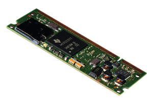
The IGEP COM AQUILA (IGEP0033-RBxx) is an industrial processor module with 256 MB RAM plus 128 MB FLASH, it is based in ARM Cortex-A8 AM335x CPU up to 1GHz with SODIMM form factor size. The next diagram shows its capabilities:
 |
Mechanical from IGEP0033:
 |
 |
Getting started
One of the most interesting parts about IGEP COM AQUILA Board is the versatility that offers to baseboard designers to implement their own specific solution. But this versatility represents too an obstacle to start developing a baseboard.
To resolve this initial obstacle, this guide does an abstract about every single part, each part is classified by:
- Power, system boot and resets
- Peripherals
Power, system boot and resets
This part can be helpful to power up and power down the full system correctly.
Power sources
Input Power sources
- VIN is the main voltage regulator that generates all the necessary internal voltages to IGEP COM AQUILA. VIN source needs 5V, read the design rules to determine the maximum current load applied.
- VBACKUP is RTC backup power supply used to keep alive the hardware clock.
Output Power sources
- VOUT is a linear regulator that offers 3V3 and 1A
- VREFP_ADC is a supply voltage used for analog digital converters.
Power sources design rules
- IGEP COM AQUILA uses a TPS73701, this LDO converts 5V (VIN input) to 3V3 (VOUT output), so you can use the following formula to calculate the maximum VIN current consumption: Ivin (maximum supply current) = 550 mA (IGEP COM AQUILA Internal maximum current) + Ivout (maximum output current).
- Read the resources detailed above to get more information.
System boot
BOOTMODE pin
- BOOTMODE is used to setup a boot priority sequence. BOOTMODE is equal to #SYS_BOOT4. It has a 100K PU signal.
More resources available at IGEP COM AQUILA Hardware Reference Manual section 6.1 and IGEP AQUILA EXPANSION Hardware Reference Manual section 5.8.
BOOTMODE design rules
- It is recommendable add a jumper header series with a 100 Ohms resistor in your base board to manage boot priority sequence. For example: If you want to reflash the internal NAND memory from microSD card you will need to unmount the jumper.
Resets
PMIC Resets
- PMIC_PWR_BTN: Drive to Low to turn off power supply (long press). Also, this pin can generate interrupts to AM335x from PMIC (short press).
More resources available at IGEP COM AQUILA Hardware Reference Manual section 6.1 and IGEP AQUILA EXPANSION Hardware Reference Manual section 5.7.
AM335x Resets
- #RESET_OUT this pin is used to reset IC from IGEP COM AQUILA like LAN8720, it is managed by AM335x.
- #POR (Power on Reset) is a cold Reset used during AM335x power-up and power-down sequence, it is managed by PMIC.
- #RESET_INis a warm Reset (also named fast reset).
More resources available at IGEP COM AQUILA Hardware Reference Manual section 6.1 and AM335x Technical Reference Manual section 8.1.7.
Resets design rules
- Resets lines are very useful to restart ICs (LDOs, Transceivers, Level shifters, etc.).
- The most priority reset is PMIC_PWR_BTN, so it is important to use at least this one.
AM335x peripherals
This part can be helpful to expand correctly the AM335x peripherals. AM335x peripherals are expanded through SODIMM 200 connector. Each bloc is classified by:
- Dedicated lines: Dedicated lines are IGEP COM AQUILA SODIMM lines designed to work with specific functionality. Change its functionality its not recommended.
- Optional lines: Optinal lines are IGEP COM AQUILA SODIMM lines designed to work with different functionalities. Change the default functionality its possible. You should revise the Mux configuration at AM335x datasheet .
Ethernet
Dedicated Ethernet
IGEP COM AQUILA uses LAN8720 Transceiver to add Ethernet communication. IGEP AQUILA EXPANSION Public Schematics adapts SODIMM lines for a RJ-45 connector.
| Name | SODIMM pin | AM335X pin |
| ETN_TXN | 19 | - |
| #ETN_LED2 | 20 | - |
| ETN_TXP | 21 | - |
| ETN_3V3 | 22 | - |
| ETN_RXN | 23 | - |
| #ETN_LED1 | 24 | - |
| ETN_RXP | 25 | - |
Ethernet design rules
- For Ethernet data lines: TX (ETN_TXN (19) and ETN_TXP(21)) and RX (ETN_RXN (23) and ETN_RXP(25))
- Maintain symmetry and isolate differential pairs from nearby signals and circuitry to mantain the signal integrity.
USBs
Dedicated USB Host
IGEP COM AQUILA uses USB1 peripheral as USB 2.0 Host. IGEP AQUILA EXPANSION Public Schematics adapts SODIMM lines for an USB Type A receptacle.
| Name | SODIMM pin | AM335X pin |
| USBH_VBUSEN | 27 | F15 |
| #USBH_OC | 28 | R13 |
| USBH_DM | 29 | R18 |
| USBH_VBUS | 30 | T18 |
| USBH_DP | 31 | R17 |
Dedicated USB OTG
IGEP COM AQUILA uses USB0 peripheral as USB 2.0 OTG. IGEP AQUILA EXPANSION Public Schematics adapts SODIMM lines for an USB Type mini AB receptacle.
| Name | SODIMM pin | AM335X pin |
| USBOTG_ID | 33 | P16 |
| USBOTG_VBUSEN | 34 | F16 |
| USBOTG_DM | 35 | N18 |
| #USBOTG_OC | 36 | V17 |
| USBOTG_DP | 37 | N17 |
| USBOTG_VBUS | 38 | P15 |
USB design rules
- For USB data lines: USB1 (USBH_DM (29) and USBH_DP (31)) and USB0 (USBOTG_DM (35) and USBOTG_DP (37))
- Maintain symmetry and isolate differential pairs from nearby signals and circuitry to mantain the signal integrity.
- VBUS overcurrent protection: USB power source current must not be pass 500mA, you should apply a protection into the baseboard. IGEP AQUILA EXPANSION Public Schematic proposes a solution using TPS2051D IC.
I2C
Dedicated I2C
IGEP COM AQUILA uses I2C0 as a dedicated I2C. I2C0 is shared with PMIC (0x2d address) and have 5K Pull ups.
| Name | SODIMM pin | AM335X pin |
| I2C0_SCL | 41 | C16 |
| I2C0_SDA | 40 | C17 |
Optional I2C
IGEP COM AQUILA contains two optional I2C buses:
| Name | SODIMM pin | AM335X pin |
| I2C1_SCL | 44 | A16 |
| I2C1_SDA | 47 | B16 |
| I2C2_SCL | 46 | B17 |
| I2C2_SDA | 48 | A17 |
I2C design rules
- I2C0 should be your default option, but it could be interesting use Optional I2Cs if your external peripheral need to use a huge transfer data connection.
- Optional I2Cs needs to be pulled up externally, 5K resistor tied to 3V3 must be necessary.
SPI
Optional SPI
IGEP COM AQUILA contains two optional SPI bus:
| Name | SODIMM pin | AM335X pin |
| SPI0_CS0 | 44 | A16 |
| SPI0_CS1 | 45 | C15 |
| SPI0_D0 | 46 | B17 |
| SPI0_D1 | 47 | B16 |
| SPI0_CLK | 48 | A17 |
| SPI1_CS0 | 60 | E15 |
| SPI1_CS1 | 59 | E16 |
| SPI1_D0 | 61 | E18 |
| SPI1_D1 | 62 | E17 |
| SPI1_CLK | 68 | H16 |
SPI design rules
- Optional SPI1 is not recommended to use, because some lines are shared with UART0 (Kernel Debug UART).
MMC
Dedicated MMC
IGEP COM AQUILA uses MMC0 from on board uSD card reader, but this pins are available into SODIMM connector too:
| Name | SODIMM pin | AM335X pin |
| MMC0_CD | 95 | A13 |
| MMC0_DAT0 | 96 | G16 |
| MMC0_DAT1 | 97 | G15 |
| MMC0_DAT2 | 98 | F18 |
| MMC0_DAT3 | 99 | F17 |
| MMC0_CMD | 100 | G18 |
| MMC0_CLK | 101 | G17 |
Optional MMC
IGEP COM AQUILA contains an optional MMC bus called MMC1:
| Name | SODIMM pin | AM335X pin |
| MMC1_CD | 51 | B13 |
| MMC1_DAT0 | 52 | K18 |
| MMC1_DAT1 | 53 | L18 |
| MMC1_DAT2 | 54 | L17 |
| MMC1_DAT3 | 55 | L16 |
| MMC1_CMD | 56 | V9 |
| MMC1_CLK | 57 | U9 |
MMC design rules
- MMC1 is not bootable during system boot process.
- MMC1 bus is a good option to expand memory capacities or use as a backup memory.
- MMC bus needs PU resistors to avoid unknown signals. 10K resistors from 3V3 source to SD1_Dx, SD1_CD and SD1_CLK must be necessary.
- Optionally: low resistance resistors could be necessary to equalize bus impedances. 10R series resistors to SD1_Dx, SD1_CD and SD1_CLK could be necessary.
UART
Optional UARTs
IGEP COM AQUILA contains six optional UARTs buses:
| Name | SODIMM pin | AM335X pin |
| UART0_TX | 59 | E16 |
| UART0_RX | 60 | E15 |
| UART0_CTS | 61 | E18 |
| UART0_RTS | 62 | E17 |
| UART1_TX | 63 | D15 |
| UART1_RX | 64 | D16 |
| UART1_CTS | 65 | D18 |
| UART1_RTS | 66 | D17 |
| UART2_TX | 52 | K18 |
| UART2_RX | 53 | L18 |
| UART3_TX | 45 | C15 |
| UART3_TX | 54 | L17 |
| UART3_RX | 55 | L16 |
| UART3_RX | 74 | C18 |
| UART4_TX | 76 | J18 |
| UART4_RX | 81 | K15 |
| UART5_TX | 67 | J17 |
| UART5_RX | 68 | H16 |
| UART5_CTS | 97 | G15 |
| UART5_RTS | 96 | G16 |
UART design rules
- IGEP COM AQUILA uses UART0 as a Kernel Debug Peripheral. This UART is a inexpensive method to detect and repair system issues. It is recommendable use another UART instead of UART0.
- UART5_RTS and UART5_CTS are shared with MMC0 (uSD card reader), don't use both at the same time. Find more information at IGEP COM AQUILA Hardware Reference Manual section 6.1
- Don't use UART3_TX and UART3_RX in both SODIMM pins
Video
Optional Video
IGEP COM AQUILA contains a LCD controller. This peripheral uses a Display Pixel Interface to transmit the information.
| Name | SODIMM pin | AM335X pin |
| LCD_D0 | 117 | U10 |
| LCD_D1 | 118 | U12 |
| LCD_D2 | 119 | V13 |
| LCD_D3 | 120 | U4 |
| LCD_D4 | 121 | V2 |
| LCD_D5 | 122 | V3 |
| LCD_D6 | 123 | V4 |
| LCD_D7 | 124 | T5 |
| LCD_D8 | 125 | T10 |
| LCD_D9 | 126 | T12 |
| LCD_D10 | 127 | T2 |
| LCD_D11 | 128 | T3 |
| LCD_D12 | 130 | T4 |
| LCD_D13 | 131 | U1 |
| LCD_D14 | 132 | U2 |
| LCD_D15 | 133 | U3 |
| LCD_D16 | 134 | T11 |
| LCD_D17 | 135 | R12 |
| LCD_D18 | 136 | U13 |
| LCD_D19 | 137 | R1 |
| LCD_D20 | 138 | R2 |
| LCD_D21 | 139 | R3 |
| LCD_D22 | 140 | R4 |
| LCD_D23 | 141 | T1 |
| LCD_HSYNC | 143 | R5 |
| LCD_VSYNC | 144 | U5 |
| LCD_OE_ACD | 145 | R6 |
| LCD_SCLK | 146 | V5 |
Video design rules
- IGEP AQUILA EXPANSION Public Schematics adapts SODIMM video lines to HDMI Transmitter.
- Optionally: low capacitance capacitors could be necessary to filter high frequency interferences. 47p capacitors tied between data lines and GND could be necessary.
- Optionally: low resistance resistors could be necessary to equalize bus impedances. 10R series resistors to data and clock lines could be necessary.
Audio
Optional Audio
IGEP COM AQUILA contains a two MCASP transceivers. This bus is can be used to attach Digital Signal Processors (DSPs), microprocessors, peripherals, and popular industry audio CODECs that implement the inter-IC sound bus standard (I2S) and Intel AC97 standard.
| Name | SODIMM pin | AM335X pin |
| MCASP0_ACLKR | 86 | B12 |
| MCASP0_ACLKX | 42 and 95 | A13 |
| MCASP0_AHCLKR | 73 | C12 |
| MCASP0_AHCLKX | 85 | A14 |
| MCASP0_AXR0 | 83 | |
| MCASP0_AXR1 | 84 | D12 |
| MCASP0_FSR | 87 | C13 |
| MCASP0_FSX | 51 | B13 |
Audio design rules
ADCs
Dedicated ADCs
| Name | SODIMM pin | AM335X pin |
| VADC | 184 | - |
| XN | 185 | B6 |
| XP | 186 | C7 |
| YN | 187 | B7 |
| YP | 188 | A7 |
| WIPER | 189 | C8 |
| ADC5 | 190 | B8 |
| ADC6 | 191 | A8 |
| ADC7 | 192 | C9 |
PWM
Optinal PWM
| Name | SODIMM pin | AM335X pin |
| EHRPWM0A | 42 and 92 | A13 |
| EHRPWM0B | 51 | B13 |
| EHRPWM2A | 117 | U10 |
| EHRPWM2B | 125 | T10 |
PWM Design rules
GPIOs
Optional GPIOs
All the optional SODIMM pins can be used as GPIOs. The following table shows some recommended SODIMMS pins to be used as GPIOs:
| Name | SODIMM pin | AM335X pin |
| KP_COL0 | 72 | U16 |
| KP_COL1 | 73 | C12 |
| KP_COL2 | 74 | C18 |
| KP_COL3 | 75 | U18 |
| KP_ROW0 | 77 | A15 |
| KP_ROW1 | 78 | D14 |
| KP_ROW2 | 79 | V12 |
| KP_ROW3 | 80 | T13 |
| GPIO0 | 148 | V14 |
| GPIO1 | 149 | U14 |
| GPIO2 | 150 | T14 |
| GPIO3 | 151 | U15 |
| GPIO5 | 153 | T16 |
| GPIO6 | 154 | V15 |
| GPIO7 | 155 | R14 |
CAN
| Name | SODIMM pin | AM335X pin |
| DCAN0_TX | 76 | J18 |
| DCAN0_RX | 81 | K15 |
| DCAN0_TX | 65 | D18 |
| DCAN0_RX | 66 | D17 |
| DCAN1_TX | 64 | D16 |
| DCAN1_RX | 63 | D15 |
| DCAN1_TX | 101 | G17 |
| DCAN1_RX | 100 | G18 |
You have successfully completed this chapter of the guide.
| |

|
If you have any question, don't ask to ask at the IGEP Community Forum or the IGEP Community Chat | 
|
Overview
This is the 1/3 chapter of IGEP AQUILA Expansion Tutorial Guide.
In this first chapter, we will learn how to connect some expansion peripherals.
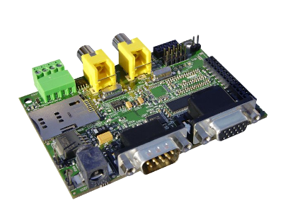
Requirements
In this tutorial we are going to use the following peripherals:
- IGEP AQUILA Expansion with its power supply
- IGEP AQUILA
- Monitor compatible with HDMI
- HDMI cable
- Network cable
- PC
| |
| |||||||||
| |
This is a work in progress article. Help other developers like you in the IGEP Community by improving it! |
Getting started
Connect IGEP AQUILA Expansion with IGEP COM AQUILA Board
The IGEP AQUILA Expansion connects to the IGEP COM AQUILA Board through K1 and J800 connectors. IGEP AQUILA Expansion should mount J101 jumper to boot from microSD card.
 |
Remote connection via Ethernet

|
If you aren't using a Linux operating system, use IGEP SDK Virtual Machine to connect to the board |
In your Host Machine, open a terminal sessions set up an Ethernet alias for your network interface,
$ sudo ifconfig eth0:0 192.168.5.10
connect to the board using the SSH protocol
$ ssh root@192.168.5.1
an empty password for root user should work to access to the shell prompt.
You have successfully completed this chapter of the guide.
| |
|
|
If you have any question, don't ask to ask at the IGEP Community Forum or the IGEP Community Chat |
|
| |
| |||||||||
Overview
This is the 2/3 chapter of IGEP AQUILA Expansion Tutorial Guide.
We will learn some basic tasks.
What can I do
How to use video HDMI
How to use audio HDMI
How to use serial console
How to use LEDs
How to use Reset Button
How to use EEPROM
How to use audio HDMI
How to use USB OTG
IGEP0033 CONNECTOR SUMMARY TABLE

|

|
| SODIMM-200
|
INTERNAL DEVICE
|
COMMENTS
| ||||||||||
| Pin
|
Type
|
Module Function
|
Dev Pin
|
MODE 0
|
MUX
|
Other MUX
|
GPIO
|
Shared
|
| |||
| 5V INPUT POWER
| ||||||||||||
| 1
|
5V
|
VIN
|
|
PMIC VCCx
|
|
|
|
2,3,4
|
4 pins are used to power the module: 1, 2, 3 and 4 PMIC is the main voltage regulator that generates all the necessary internal voltages. TEXAS INSTRUMENTS P/N: TPS65910A3A1RSL
| |||
| 2
|
5V
|
VIN
|
|
PMIC VCCx
|
|
|
|
1,3,4
| ||||
| 3
|
5V
|
VIN
|
|
PMIC VCCx
|
|
|
|
1,2,4
| ||||
| 4
|
5V
|
VIN
|
|
PMIC VCCx
|
|
|
|
1,2,3
| ||||
| 3V3 OUTPUT POWER
| ||||||||||||
| 5
|
3V3
|
VOUT
|
|
PMIC2 VOUT
|
|
|
|
6,7,9,10,11,12
|
7 pins are used to output 3V3 voltage / 1A for a base board 5,6,7,9,10,11,12
| |||
| 6
|
3V3
|
VOUT
|
|
PMIC2 VOUT
|
|
|
|
5,6,9,10,11,12
| ||||
| 7
|
3V3
|
VOUT
|
|
PMIC2 VOUT
|
|
|
|
5,6,9,10,11,12
| ||||
| BOOT MODE
| ||||||||||||
| 8
|
IN
|
BOOTMODE
|
T1
|
#LCD_DATA4
|
|
GPMC_A4
|
GPIO2_10
|
141
|
BOOT mode select H: from NAND / L: from UART/USB
| |||
| 3V3 OUTPUT POWER
| ||||||||||||
| 9
|
3V3
|
VOUT
|
|
PMIC2 VOUT
|
|
|
|
5,6,7,10,11,12
|
PMIC2 is a linear regulator that supply 3V3 / 1A TEXAS INSTRUMENTS P/N: TPS73701
| |||
| 10
|
3V3
|
VOUT
|
|
PMIC2 VOUT
|
|
|
|
5,6,7,9,11,12
| ||||
| 11
|
3V3
|
VOUT
|
|
PMIC2 VOUT
|
|
|
|
5,6,7,9,10,12
| ||||
| 12
|
3V3
|
VOUT
|
|
PMIC2 VOUT
|
|
|
|
5,6,7,9,10,11
| ||||
| CONTROL SIGNALS
| ||||||||||||
| 13
|
VK
|
VBACKUP
|
27
|
PMIC VBACKUP
|
|
|
|
|
RTC backup power supply. Connect to a 3V1 coin cell battery
| |||
| 14
|
IN
|
PMIC_PWR_BTN
|
33
|
PMIC PWRON
|
|
|
|
|
Power ON Button. Drive to Low to turn off power supply. Refer to PMIC Manual
| |||
| 15
|
OUT
|
#RESET_OUT
|
B14
|
EMU1
|
|
-
|
GPIO3_8
|
|
Active Low Reset Out. Connected to the onboard LAN8720-pin15
| |||
| 16
|
IN
|
#POR
|
B15
|
PWRONRSTn
|
|
-
|
-
|
|
Power ON Reset. Active Low
| |||
| 17
|
IO
|
#RESET_IN
|
A10
|
WARMRSTn
|
|
-
|
-
|
|
Warm Reset. Refer to AM335x Technical Reference Manual
| |||
| 18
|
GND
|
GND
|
|
|
|
|
|
|
Power Ground
| |||
| ETHERNET
| ||||||||||||
| 19
|
ETH
|
ETN_TXN
|
20
|
LAN8720 TXN
|
|
|
|
|
Analog Transmit Data Negative. Differential output to magnetics
| |||
| 20
|
OUT
|
#ETN_LED2
|
2
|
LAN8720 #LED2
|
|
|
|
|
Active Low. LED2 Yellow means 100Mbps speed. Inactive if 10Mbps or line isolation
| |||
| 21
|
ETH
|
ETN_TXP
|
21
|
LAN8720 TXP
|
|
|
|
|
Analog Transmit Data Positive. Differential output to magnetics
| |||
| 22
|
3V3
|
ETN_3V3
|
4
|
PMIC VAUX33
|
|
|
|
|
3V3 to magnetics
| |||
| 23
|
ETH
|
ETN_RXN
|
22
|
LAN8720 RXN
|
|
|
|
|
Analog Receive Data Negative. Differential output to magnetics
| |||
| 24
|
OUT
|
#ETN_LED1
|
3
|
LAN8720 #LED1
|
|
|
|
|
Active Low. LED1 Green indicates valid link and blinks when there is activity
| |||
| 25
|
ETH
|
ETN_RXP
|
23
|
LAN8720 RXP
|
|
|
|
|
Analog Receive Data Poitive. Differential output to magnetics
| |||
| 26
|
GND
|
GND
|
|
|
|
|
|
|
Power Ground
| |||
| USB HOST
| ||||||||||||
| 27
|
OUT
|
USBH_VBUSEN
|
F15
|
USB1_DRVVBUS
|
|
-
|
GPIO3_13
|
|
Active High. Enables external VBUS power supply
| |||
| 28
|
IN
|
#USBH_OC
|
F16
|
USB0_DRVVBUS
|
|
-
|
GPIO0_18
|
|
Active Low. Over current indication to module
| |||
| 29
|
USB
|
USBH_DM
|
R18
|
USB1_DM
|
|
-
|
-
|
|
Analog D- data pin of the USB cable
| |||
| 30
|
USB
|
USBH_VBUS
|
T18
|
USB1_VBUS
|
|
-
|
-
|
|
VBUS pin of the USB cable. Used for the VBUS comparator inputs
| |||
| 31
|
USB
|
USBH_DP
|
R17
|
USB1_DP
|
|
-
|
-
|
|
Analog D+ data pin of the USB cable
| |||
| 32
|
GND
|
GND
|
|
|
|
|
|
|
Power Ground
| |||
| | ||||||||||||
| | ||||||||||||
K100 SODIMM 200 connector
|
SODIMM-200 |
INTERNAL DEVICE |
COMMENTS | ||||||||||
|
Pin |
Type |
Module Function |
Dev Pin |
MODE 0 |
MUX |
Other MUX |
GPIO |
Shared |
||||
|
5V INPUT POWER | ||||||||||||
|
1 |
5V |
VIN |
PMIC VCCx |
2,3,4 |
4 pins are used to power the module: 1, 2, 3 and 4 PMIC is the main voltage regulator that generates all the necessary internal voltages. TEXAS INSTRUMENTS P/N: TPS65910A3A1RSL | |||||||
|
2 |
5V |
VIN |
PMIC VCCx |
1,3,4 | ||||||||
|
3 |
5V |
VIN |
PMIC VCCx |
1,2,4 | ||||||||
|
4 |
5V |
VIN |
PMIC VCCx |
1,2,3 | ||||||||
|
3V3 OUTPUT POWER | ||||||||||||
|
5 |
3V3 |
VOUT |
PMIC2 VOUT |
6,7,9,10,11,12 |
7 pins are used to output 3V3 voltage / 1A for a base board 5,6,7,9,10,11,12 | |||||||
|
6 |
3V3 |
VOUT |
PMIC2 VOUT |
5,6,9,10,11,12 | ||||||||
|
7 |
3V3 |
VOUT |
PMIC2 VOUT |
5,6,9,10,11,12 | ||||||||
|
BOOT MODE | ||||||||||||
|
8 |
IN |
BOOTMODE |
T1 |
#LCD_DATA4 |
GPMC_A4 |
GPIO2_10 |
141 |
BOOT mode select H: from NAND / L: from UART/USB | ||||
|
3V3 OUTPUT POWER | ||||||||||||
|
9 |
3V3 |
VOUT |
PMIC2 VOUT |
5,6,7,10,11,12 |
PMIC2 is a linear regulator that supply 3V3 / 1A TEXAS INSTRUMENTS P/N: TPS73701 | |||||||
|
10 |
3V3 |
VOUT |
PMIC2 VOUT |
5,6,7,9,11,12 | ||||||||
|
11 |
3V3 |
VOUT |
PMIC2 VOUT |
5,6,7,9,10,12 | ||||||||
|
12 |
3V3 |
VOUT |
PMIC2 VOUT |
5,6,7,9,10,11 | ||||||||
|
CONTROL SIGNALS | ||||||||||||
|
13 |
VK |
VBACKUP |
27 |
PMIC VBACKUP |
RTC backup power supply. Connect to a 3V1 coin cell battery | |||||||
|
14 |
IN |
PMIC_PWR_BTN |
33 |
PMIC PWRON |
Power ON Button. Drive to Low to turn off power supply. Refer to PMIC Manual | |||||||
|
15 |
OUT |
#RESET_OUT |
B14 |
EMU1 |
- |
GPIO3_8 |
Active Low Reset Out. Connected to the onboard LAN8720-pin15 | |||||
|
16 |
IN |
#POR |
B15 |
PWRONRSTn |
- |
- |
Power ON Reset. Active Low | |||||
|
17 |
IO |
#RESET_IN |
A10 |
WARMRSTn |
- |
- |
Warm Reset. Refer to AM335x Technical Reference Manual | |||||
|
18 |
GND |
GND |
Power Ground | |||||||||
|
ETHERNET | ||||||||||||
|
19 |
ETH |
ETN_TXN |
20 |
LAN8720 TXN |
Analog Transmit Data Negative. Differential output to magnetics | |||||||
|
20 |
OUT |
#ETN_LED2 |
2 |
LAN8720 #LED2 |
Active Low. LED2 Yellow means 100Mbps speed. Inactive if 10Mbps or line isolation | |||||||
|
21 |
ETH |
ETN_TXP |
21 |
LAN8720 TXP |
Analog Transmit Data Positive. Differential output to magnetics | |||||||
|
22 |
3V3 |
ETN_3V3 |
4 |
PMIC VAUX33 |
3V3 to magnetics | |||||||
|
23 |
ETH |
ETN_RXN |
22 |
LAN8720 RXN |
Analog Receive Data Negative. Differential output to magnetics | |||||||
|
24 |
OUT |
#ETN_LED1 |
3 |
LAN8720 #LED1 |
Active Low. LED1 Green indicates valid link and blinks when there is activity | |||||||
|
25 |
ETH |
ETN_RXP |
23 |
LAN8720 RXP |
Analog Receive Data Poitive. Differential output to magnetics | |||||||
|
26 |
GND |
GND |
Power Ground | |||||||||
|
USB HOST | ||||||||||||
|
27 |
OUT |
USBH_VBUSEN |
F15 |
USB1_DRVVBUS |
- |
GPIO3_13 |
Active High. Enables external VBUS power supply | |||||
|
28 |
IN |
#USBH_OC |
F16 |
USB0_DRVVBUS |
- |
GPIO0_18 |
Active Low. Over current indication to module | |||||
|
29 |
USB |
USBH_DM |
R18 |
USB1_DM |
- |
- |
Analog D- data pin of the USB cable | |||||
|
30 |
USB |
USBH_VBUS |
T18 |
USB1_VBUS |
- |
- |
VBUS pin of the USB cable. Used for the VBUS comparator inputs | |||||
|
31 |
USB |
USBH_DP |
R17 |
USB1_DP |
- |
- |
Analog D+ data pin of the USB cable | |||||
|
32 |
GND |
GND |
Power Ground | |||||||||
|
USB OTG | ||||||||||||
|
33 |
USB |
USBOTG_ID |
P16 |
USB0_ID |
- |
- |
ID pin of the USB cable. A-device is grounded; B-device is floating | |||||
|
34 |
OUT |
USBOTG_VBUSEN |
R13 |
GPMC_A0 |
GPIO1_16 |
GPMC_A16 |
GPIO1_16 |
156 |
Active High. Enables external VBUS power supply | |||
|
35 |
USB |
USBOTG_DM |
N18 |
USB0_DM |
- |
- |
Analog D- data pin of the USB cable | |||||
|
36 |
IN |
#USBOTG_OC |
V17 |
GPMC_A11 |
GPIO1_27 |
GPMC_A27 |
GPIO1_27 |
152 |
Active Low. Over current indication to module | |||
|
37 |
USB |
USBOTG_DP |
N17 |
USB0_DP |
- |
- |
Analog D+ data pin of the USB cable | |||||
|
38 |
IN |
USBOTG_VBUS |
P15 |
USB0_VBUS |
- |
- |
VBUS pin of the USB cable. Used for the VBUS comparator inputs | |||||
|
39 |
GND |
GND |
Power Ground | |||||||||
|
I2C INTERFACE | ||||||||||||
|
40 |
IO |
I2C_DATA |
C17 |
I2C0_SDA |
TIMER4 |
GPIO3_5 |
PMIC pin 8 |
I2C bus data. Shared device on this bus and address: PMIC @2D (HEXA) | ||||
|
41 |
IO |
I2C_CLK |
C16 |
I2C0_SCL |
TIMER7 |
GPIO3_6 |
PMIC pin 9 |
I2C bus clock | ||||
|
PWM | ||||||||||||
|
42 |
OUT |
PWM |
A13 |
MCASP0_ACLKX |
EHRPWM0A |
MMC0_SDCD |
GPIO3_14 |
95 & sd_cd |
PWM Output. Shared internally with SD CD. Configured by default as MMC0_SDCD | |||
|
OWIRE: ONE WIRE INTERFACE | ||||||||||||
|
43 |
IO |
OWDAT |
V14 |
GPMC_A1 |
GPIO1_17 |
GPMC_A17 |
GPIO1_17 |
148 |
AM335x has not 1-wire controller. GPIO1_17 is used. Requires pull up. | |||
|
CSPI: SERIAL PERIPHERAL INTERFACE | ||||||||||||
|
44 |
OUT |
CSPI_SS0 |
A16 |
SPI0_CS0 |
I2C1_SCL |
GPIO0_5 |
SPI Slave select signal | |||||
|
45 |
OUT |
CSPI_SS1 |
C15 |
SPI0_CS1 |
UART3_RXD |
GPIO0_6 |
SPI Slave select signal | |||||
|
46 |
OUT |
CSPI_MOSI |
B17 |
SPI0_D0 |
I2C2_SCL |
GPIO0_3 |
SPI Master Output-Slave Input | |||||
|
47 |
IN |
CSPI_MISO |
B16 |
SPI0_D1 |
I2C1_SDA |
GPIO0_4 |
SPI Master Input-Slave Output | |||||
|
48 |
OUT |
CSPI_SCLK |
A17 |
SPI0_SCLK |
I2C2_SDA |
GPIO0_2 |
SPI Clock | |||||
|
49 |
OUT |
CSPI_RDY |
Not connected | |||||||||
|
50 |
GND |
GND |
Power Ground | |||||||||
|
uSD1: SECURE DIGITAL INTERFACE 1 | ||||||||||||
|
51 |
IN |
SD1_CD |
B13 |
MCASP0_FSX |
MMC1_SDCD |
EHRPWM0B |
GPIO3_15 |
SD CARD Detect | ||||
|
52 |
IO |
SD1_D0 |
K18 |
MII1_TX_CLK |
MMC1_DAT0 |
UART2_RXD |
GPIO3_9 |
SD Data 0 bidirectional. User must pull up this signal accordingly | ||||
|
53 |
IO |
SD1_D1 |
L18 |
MII1_RX_CLK |
MMC1_DAT1 |
UART2_TXD |
GPIO3_10 |
SD Data 1 bidirectional. User must pull up this signal accordingly | ||||
|
54 |
IO |
SD1_D2 |
L17 |
MII1_RXD3 |
MMC1_DAT2 |
UART3_RXD |
GPIO2_18 |
SD Data 2 bidirectional. User must pull up this signal accordingly | ||||
|
55 |
IO |
SD1_D3 |
L16 |
MII1_RXD2 |
MMC1_DAT3 |
UART3_TXD |
GPIO2_19 |
SD Data 3 bidirectional. User must pull up this signal accordingly | ||||
|
56 |
IO |
SD1_CMD |
V9 |
GPMC_CSn2 |
MMC1_CMD |
GPMC_BE1N |
GPIO1_31 |
SD command bidirectional data | ||||
|
57 |
IO |
SD1_CLK |
U9 |
GPMC_CSn1 |
MMC1_CLK |
GPMC_CLK |
GPIO1_30 |
SD Output clock | ||||
|
58 |
GND |
GND |
Power Ground | |||||||||
|
1ST UART | ||||||||||||
|
59 |
OUT |
UART1_TXD |
E16 |
UART0_TXD |
SPI1_CS1 |
GPIO1_11 |
Debug UART Transmit Data Output | |||||
|
60 |
IN |
UART1_RXD |
E15 |
UART0_RXD |
SPI1_CS0 |
GPIO1_10 |
Debug UART Receive Data Intput | |||||
|
61 |
IN |
UART1_RTS/CTS IN |
E18 |
UART0_CTSn |
SPI1_D0 |
GPIO1_8 |
Debug UART RTS/CTS INPUT | |||||
|
62 |
OUT |
UART1_CTS/RTS OUT |
E17 |
UART0_RTSn |
SPI1_D1 |
GPIO1_9 |
Debug UART RTS/CTS OUTPUT | |||||
|
2ND UART | ||||||||||||
|
63 |
OUT |
UART2_TXD |
D15 |
UART1_TXD |
DCAN1_RX |
GPIO0_15 |
UART Transmit Data Output | |||||
|
64 |
IN |
UART2_RXD |
D16 |
UART1_RXD |
DCAN1_TX |
GPIO0_14 |
UART Receive Data Intput | |||||
|
65 |
IN |
UART2_RTS/CTS IN |
D18 |
UART1_CTSn |
DCAN0_TX |
GPIO0_12 |
UART RTS/CTS INPUT | |||||
|
66 |
OUT |
UART2_CTS/RTS OUT |
D17 |
UART1_RTSn |
DCAN0_RX |
GPIO0_13 |
UART RTS/CTS OUTPUT | |||||
|
3RD UART | ||||||||||||
|
67 |
OUT |
UART3_TXD |
J17 |
MII1_RX_DV |
UART5_TXD |
MMC2_DAT0 |
GPIO3_4 |
UART Transmit Data Output | ||||
|
68 |
IN |
UART3_RXD |
H16 |
MII1_COL |
UART5_RXD |
SPI1_SCLK |
GPIO3_0 |
UART Receive Data Intput | ||||
|
69 |
IN |
UART3_RTS/CTS IN |
G15 |
MMC0_DAT1 |
UART5_CTSN |
UART3_RXD |
GPIO2_28 |
97 & sd_d1 |
UART RTS/CTS INPUT. Shared with internal SD D1. Configured as MMC0_DAT1 | |||
|
70 |
OUT |
UART3_CTS/RTS OUT |
G16 |
MMC0_DAT0 |
UART5_RTSN |
UART3_TXD |
GPIO2_29 |
96 & sd_d0 |
UART RTS/CTS OUTPUT. Shared with internal SD D0. Configured as MMC0_DAT0 | |||
|
71 |
GND |
GND |
Power Ground | |||||||||
|
KEYPAD / CAN | ||||||||||||
|
72 |
IN |
KP_COL0 |
U16 |
GPMC_A9 |
GPIO1_25 |
GPMC_A25 |
GPIO1_25 |
159 |
KeyPAD Column 0. Pin shared with SODIMM pin 159 | |||
|
73 |
IN |
KP_COL1 |
C12 |
MCASP0_AHCLKR |
GPIO3_17 |
EHRPWM0_SYNCI |
GPIO3_17 |
KeyPAD Column 1 | ||||
|
74 |
IN |
KP_COL2 |
C18 |
ECAP0_IN_PWM0_OUT |
GPIO0_7 |
UART3_TXD |
GPIO0_7 |
KeyPAD Column 2 | ||||
|
75 |
IN |
KP_COL3 |
U18 |
GPMC_BEn1 |
GPIO1_28 |
GPMC_DIR |
GPIO1_28 |
KeyPAD Column 3 | ||||
|
76 |
OUT |
TXCAN |
J18 |
MII1_TXD3 |
DCAN0_TX |
UART4_RXD |
GPIO0_16 |
CAN Transmission line | ||||
|
77 |
IN |
KP_ROW0 |
A15 |
XDMA_EVENT_INTR0 |
GPIO0_19 |
TIMER4 |
GPIO0_19 |
KeyPAD Row 0 | ||||
|
78 |
IN |
KP_ROW1 |
D14 |
XDMA_EVENT_INTR1 |
GPIO0_20 |
TIMER7 |
GPIO0_20 |
KeyPAD Row 1 | ||||
|
79 |
IN |
KP_ROW2 |
V12 |
GPMC_CLK |
GPIO2_1 |
MMC2_CLK |
GPIO2_1 |
KeyPAD Row 2 | ||||
|
80 |
IN |
KP_ROW3 |
T13 |
GPMC_CSn3 |
GPIO2_0 |
MMC2_CMD |
GPIO2_0 |
KeyPAD Row 3 | ||||
|
81 |
IN |
RXCAN |
K15 |
MII1_TXD2 |
DCAN0_RX |
UART4_TXD |
GPIO0_17 |
CAN Reception line | ||||
|
82 |
GND |
GND |
Power Ground | |||||||||
|
SSI 1: SERIAL AUDIO PORT 1 | ||||||||||||
|
83 |
IO |
SSI1_INT |
D12 |
MCASP0_AXR0 |
GPIO3_16 |
MMC2_SDCD |
GPIO3_16 |
Serial Audio Interface Interrupt signal | ||||
|
84 |
IO |
SSI1_RXD |
D13 |
MCASP0_AXR1 |
MCASP1_AXR0 |
EMU3 |
GPIO3_20 |
Serial Audio Interface serial data line 0 | ||||
|
85 |
IO |
SSI1_TXD |
A14 |
MCASP0_AHCLKX |
MCASP1_AXR1 |
EMU4 |
GPIO3_21 |
Serial Audio Interface serial data line 1 | ||||
|
86 |
IO |
SSI1_CLK |
B12 |
MCASP0_ACLKR |
MCASP1_ACLKX |
MMC0_SDWP |
GPIO3_18 |
Serial Audio Interface serial clock | ||||
|
87 |
IO |
SSI1_FS |
C13 |
MCASP0_FSR |
MCASP1_FSX |
EMU2 |
GPIO3_19 |
Serial Audio Interface left/right clock | ||||
|
88 |
GND |
GND |
Power Ground | |||||||||
|
SSI 2: SERIAL AUDIO PORT 2 | ||||||||||||
|
89 |
SSI2_INT |
Not connected | ||||||||||
|
90 |
SSI2_RXD |
Not connected | ||||||||||
|
91 |
SSI2_TXD |
Not connected | ||||||||||
|
92 |
SSI2_CLK |
Not connected | ||||||||||
|
93 |
SSI2_FS |
Not connected | ||||||||||
|
94 |
GND |
GND |
Power Ground | |||||||||
|
uSD2: SECURE DIGITAL INTERFACE 2 | ||||||||||||
|
95 |
IN |
SD2_CD |
A13 |
MCASP0_ACLKX |
MMC0_SDCD |
EHRPWM0A |
GPIO3_14 |
42 & sd_cd |
SD Card detect. Shared internally with SD CD. It can be configured as PWM output | |||
|
96 |
IO |
SD2_D0 |
G16 |
MMC0_DAT0 |
UART5_RTSN |
GPIO2_29 |
70 & sd_d0 |
SD Data 1 bidirectional. Shared internally with SD D0. It can be configured as UART_RTSN | ||||
|
97 |
IO |
SD2_D1 |
G15 |
MMC0_DAT1 |
UART5_CTSN |
GPIO2_28 |
69 & sd_d1 |
SD Data 1 bidirectional. Shared internally with SD D1. It can be configured as UART_CTSN | ||||
|
98 |
IO |
SD2_D2 |
F18 |
MMC0_DAT2 |
TIMER6 |
GPIO2_27 |
sd_d2 |
SD Data 2 bidirectional. Shared internally with SD D2 | ||||
|
99 |
IO |
SD2_D3 |
F17 |
MMC0_DAT3 |
TIMER5 |
GPIO2_26 |
sd_d3 |
SD Data 3 bidirectional. Shared internally with SD D3 | ||||
|
100 |
IO |
SD2_CMD |
G18 |
MMC0_CMD |
DCAN1_RX |
GPIO2_31 |
sd_cmd |
SD CMD bidirectional. Shared internally with SD CMD | ||||
|
101 |
SD2_CLK |
G17 |
MMC0_CLK |
DCAN1_TX |
GPIO2_30 |
sd_clk |
SD Clock bidirectional. Shared internally with SD CK | |||||
|
102 |
GND |
GND |
Power Ground | |||||||||
|
CMOS SENSOR INTERFACE | ||||||||||||
|
103 |
CSI_D0 |
Not connected | ||||||||||
|
104 |
CSI_D1 |
Not connected | ||||||||||
|
105 |
CSI_D2 |
Not connected | ||||||||||
|
106 |
CSI_D3 |
Not connected | ||||||||||
|
107 |
CSI_D4 |
Not connected | ||||||||||
|
108 |
CSI_D5 |
Not connected | ||||||||||
|
109 |
CSI_D6 |
Not connected | ||||||||||
|
110 |
CSI_D7 |
Not connected | ||||||||||
|
111 |
GND |
GND |
Power Ground | |||||||||
|
112 |
CSI_HSYNC |
Not connected | ||||||||||
|
113 |
CSI_VSYNC |
Not connected | ||||||||||
|
114 |
CSI_PIXCLK |
Not connected | ||||||||||
|
115 |
CSI_MCLK |
Not connected | ||||||||||
|
116 |
GND |
GND |
Power Ground | |||||||||
|
LCD CONTROLLER | ||||||||||||
|
117 |
OUT |
LCD_D0 |
U10 |
GPMC_AD8 |
LCD_DATA23 |
EHRPWM2A |
GPIO0_22 |
LCD DATA BUS | ||||
|
118 |
OUT |
LCD_D1 |
U12 |
GPMC_AD11 |
LCD_DATA20 |
MMC2_DAT7 |
GPIO0_27 |
LCD DATA BUS | ||||
|
119 |
OUT |
LCD_D2 |
V13 |
GPMC_AD14 |
LCD_DATA17 |
MMC2_DAT2 |
GPIO1_14 |
LCD DATA BUS | ||||
|
120 |
IO |
LCD_D3 |
U4 |
LCD_DATA11 |
GPMC_A15 |
GPIO2_17 |
LCD DATA BUS / SYS_BOOT11 | |||||
|
121 |
IO |
LCD_D4 |
V2 |
LCD_DATA12 |
GPMC_A16 |
GPIO0_8 |
LCD DATA BUS / SYS_BOOT12 | |||||
|
122 |
IO |
LCD_D5 |
V3 |
LCD_DATA13 |
GPMC_A17 |
GPIO0_9 |
LCD DATA BUS / SYS_BOOT13 | |||||
|
123 |
IO |
LCD_D6 |
V4 |
LCD_DATA14 |
GPMC_A18 |
GPIO0_10 |
LCD DATA BUS / SYS_BOOT14 | |||||
|
124 |
IO |
LCD_D7 |
T5 |
LCD_DATA15 |
GPMC_A19 |
GPIO0_11 |
LCD DATA BUS / SYS_BOOT15 | |||||
|
125 |
OUT |
LCD_D8 |
T10 |
GPMC_AD9 |
LCD_DATA22 |
EHRPWM2B |
GPIO0_23 |
LCD DATA BUS | ||||
|
126 |
OUT |
LCD_D9 |
T12 |
GPMC_AD12 |
LCD_DATA19 |
MMC2_DAT0 |
GPIO1_12 |
LCD DATA BUS | ||||
|
127 |
IO |
LCD_D10 |
T2 |
LCD_DATA5 |
GPMC_A5 |
GPIO2_11 |
LCD DATA BUS / SYS_BOOT5 | |||||
|
128 |
OUT |
LCD_D11 |
T3 |
LCD_DATA6 |
GPMC_A6 |
GPIO2_12 |
LCD DATA BUS / SYS_BOOT6 | |||||
|
129 |
GND |
GND |
Power Ground | |||||||||
|
130 |
IO |
LCD_D12 |
T4 |
LCD_DATA7 |
GPMC_A7 |
GPIO2_13 |
LCD DATA BUS / SYS_BOOT7 | |||||
|
131 |
IO |
LCD_D13 |
U1 |
LCD_DATA8 |
GPMC_A12 |
GPIO2_14 |
LCD DATA BUS / SYS_BOOT8 | |||||
|
132 |
IO |
LCD_D14 |
U2 |
LCD_DATA9 |
GPMC_A13 |
GPIO2_15 |
LCD DATA BUS / SYS_BOOT9 | |||||
|
133 |
IO |
LCD_D15 |
U3 |
LCD_DATA10 |
GPMC_A14 |
GPIO2_16 |
LCD DATA BUS / SYS_BOOT10 | |||||
|
134 |
OUT |
LCD_D16 |
T11 |
GPMC_AD10 |
LCD_DATA21 |
MMC2_DAT6 |
GPIO0_26 |
LCD DATA BUS | ||||
|
135 |
OUT |
LCD_D17 |
R12 |
GPMC_AD13 |
LCD_DATA18 |
MMC2_DAT1 |
GPIO1_13 |
LCD DATA BUS | ||||
|
136 |
OUT |
LCD_D18 |
U13 |
GPMC_AD15 |
LCD_DATA16 |
MMC2_DAT3 |
GPIO1_15 |
LCD DATA BUS | ||||
|
137 |
IO |
LCD_D19 |
R1 |
LCD_DATA0 |
GPMC_A0 |
GPIO2_6 |
JTAG7 |
LCD DATA BUS / SYS_BOOT0 | ||||
|
138 |
IO |
LCD_D20 |
R2 |
LCD_DATA1 |
GPMC_A1 |
GPIO2_7 |
JTAG5 |
LCD DATA BUS / SYS_BOOT1 | ||||
|
139 |
IO |
LCD_D21 |
R3 |
LCD_DATA2 |
GPMC_A2 |
GPIO2_8 |
LCD DATA BUS / SYS_BOOT2 | |||||
|
140 |
IO |
LCD_D22 |
R4 |
LCD_DATA3 |
GPMC_A3 |
GPIO2_9 |
LCD DATA BUS / SYS_BOOT3 | |||||
|
141 |
IO |
LCD_D23 |
T1 |
LCD_DATA4 |
GPMC_A4 |
GPIO2_10 |
8 |
LCD DATA BUS / SYS_BOOT4 | ||||
|
142 |
GND |
GND |
Power Ground | |||||||||
|
143 |
OUT |
LCD_HSYNC |
R5 |
LCD_HSYNC |
GPMC_A9 |
GPIO2_23 |
LCD BUS HORIZONTAL SYNCHRONISM | |||||
|
144 |
OUT |
LCD_VSYNC |
U5 |
LCD_VSYNC |
GPMC_A8 |
GPIO2_22 |
LCD BUS VERTICAL SYNCHRONISM | |||||
|
145 |
OUT |
LCD_OE_ACD |
R6 |
LCD_AC_BIAS_EN |
GPMC_A11 |
GPIO2_25 |
LCD BUS CONTROL | |||||
|
146 |
OUT |
LCD_SCLK |
V5 |
LCD_PCLK |
GPMC_A10 |
GPIO2_24 |
LCD BUS CLOCK | |||||
|
147 |
GND |
GND |
Power Ground | |||||||||
|
IGEPTM COM CYGNUS and IGEPTM COM AQUILA MODULES SPECIFIC SIGNALS | ||||||||||||
|
148 |
IO |
GPIO0 |
V14 |
GPMC_A1 |
GPIO1_17 |
GPMC_A17 |
GPIO1_17 |
43 |
I/O SHARED WITH SODIMM pin 43 OWDAT one wire | |||
|
149 |
IO |
GPIO1 |
U14 |
GPMC_A2 |
GPIO1_18 |
GPMC_A18 |
GPIO1_18 |
I/O | ||||
|
150 |
IO |
GPIO2 |
T14 |
GPMC_A3 |
GPIO1_19 |
GPMC_A19 |
GPIO1_19 |
I/O | ||||
|
151 |
IO |
GPIO3 |
U15 |
GPMC_A6 |
GPIO1_22 |
GPMC_A22 |
GPIO1_22 |
I/O | ||||
|
152 |
IO |
GPIO4 |
V17 |
GPMC_A11 |
GPIO1_27 |
GPMC_A27 |
GPIO1_27 |
36 |
I/O SHARED WITH SODIMM pin 36 #USBOTG_OC | |||
|
153 |
IO |
GPIO5 |
T16 |
GPMC_A10 |
GPIO1_26 |
GPMC_A26 |
GPIO1_26 |
I/O | ||||
|
154 |
IO |
GPIO6 |
V15 |
GPMC_A5 |
GPIO1_21 |
GPMC_A21 |
GPIO1_21 |
I/O | ||||
|
155 |
IO |
GPIO7 |
R14 |
GPMC_A4 |
GPIO1_20 |
GPMC_A20 |
GPIO1_20 |
I/O | ||||
|
156 |
IO |
GPIO8 |
R13 |
GPMC_A0 |
GPIO1_16 |
GPMC_A16 |
GPIO1_16 |
34 |
I/O SHARED WITH SODIMM pin 34 USBOTG_VBUSEN | |||
|
157 |
IO |
GPIO9 |
T15 |
GPMC_A7 |
GPIO1_23 |
GPMC_A23 |
GPIO1_23 |
USER LED |
I/O SHARED WITH USER LED | |||
|
158 |
IO |
GPIO10 |
V16 |
GPMC_A8 |
GPIO1_24 |
GPMC_A24 |
GPIO1_24 |
PMIC pin37 |
I/O SHARED WITH REGULATOR SLEEP | |||
|
159 |
IO |
GPIO11 |
U16 |
GPMC_A9 |
GPIO1_25 |
GPMC_A25 |
GPIO1_25 |
72 |
I/O SHARED WITH SODIMM pin 72 KEYCOL0 | |||
|
160 |
GND |
GND |
Power Ground | |||||||||
|
161 |
OUT |
GPMC_WPn |
U17 |
GPMC_WPn |
GPMC_CSN5 |
GPIO0_31 |
NAND |
SHARED WITH NAND FLASH MEMORY WPN | ||||
|
162 |
NC |
Not connected | ||||||||||
|
163 |
NC |
Not connected | ||||||||||
|
164 |
NC |
Not connected | ||||||||||
|
165 |
NC |
Not connected | ||||||||||
|
166 |
NC |
Not connected | ||||||||||
|
167 |
NC |
Not connected | ||||||||||
|
168 |
NC |
Not connected | ||||||||||
|
169 |
NC |
Not connected | ||||||||||
|
170 |
NC |
Not connected | ||||||||||
|
171 |
GND |
GND |
Power Ground | |||||||||
|
172 |
NC |
Not connected | ||||||||||
|
173 |
NC |
Not connected | ||||||||||
|
174 |
NC |
Not connected | ||||||||||
|
175 |
NC |
Not connected | ||||||||||
|
176 |
NC |
Not connected | ||||||||||
|
177 |
NC |
Not connected | ||||||||||
|
178 |
NC |
Not connected | ||||||||||
|
179 |
OUT |
GPMC_BEn0_CLE |
T6 |
GPMC_BEn0_CLE |
TIMER5 |
GPIO2_5 |
NAND |
SHARED WITH NAND FLASH MEMORY | ||||
|
180 |
OUT |
GPMC_ADVn_ALE |
R7 |
GPMC_ADVn_ALE |
TIMER4 |
GPIO2_2 |
NAND |
SHARED WITH NAND FLASH MEMORY | ||||
|
181 |
OUT |
GPMC_WEn |
U6 |
GPMC_WEn |
TIMER6 |
GPIO2_4 |
NAND |
SHARED WITH NAND FLASH MEMORY | ||||
|
182 |
OUT |
GPMC_OEn_REn |
T7 |
GPMC_OEn_REn |
TIMER7 |
GPIO2_3 |
NAND |
SHARED WITH NAND FLASH MEMORY | ||||
|
183 |
GND |
GND_ADC |
E8 |
VSSA_ADC |
Analog Ground | |||||||
|
184 |
NC |
Not connected | ||||||||||
|
185 |
ADC |
XN |
B6 |
AIN0 |
- |
- |
TOUCHSCREEN ADC INPUT CHANNEL | |||||
|
186 |
ADC |
XP |
C7 |
AIN1 |
- |
- |
TOUCHSCREEN ADC INPUT CHANNEL | |||||
|
187 |
ADC |
YN |
B7 |
AIN2 |
- |
- |
TOUCHSCREEN ADC INPUT CHANNEL | |||||
|
188 |
ADC |
YP |
A7 |
AIN3 |
- |
- |
TOUCHSCREEN ADC INPUT CHANNEL | |||||
|
189 |
ADC |
WIPER |
C8 |
AIN4 |
- |
- |
TOUCHSCREEN ADC INPUT CHANNEL | |||||
|
190 |
ADC |
ADC5 |
B8 |
AIN5 |
- |
- |
GENERAL PURPOSE ADC CHANNEL | |||||
|
191 |
ADC |
ADC6 |
A8 |
AIN6 |
- |
- |
GENERAL PURPOSE ADC CHANNEL | |||||
|
192 |
ADC |
ADC7 |
C9 |
AIN7 |
- |
- |
GENERAL PURPOSE ADC CHANNEL | |||||
|
193 |
IN |
WAKEUP |
C5 |
EXT_WAKEUP |
- |
- |
EXTERNAL WAKE UP | |||||
|
194 |
NC |
Not connected | ||||||||||
|
195 |
NC |
Not connected | ||||||||||
|
196 |
NC |
Not connected | ||||||||||
|
197 |
IO |
- |
C14 |
EMU0 |
GPIO3_7 |
- |
GPIO3_7 |
|||||
|
198 |
OUT |
MDC |
M18 |
MDIO_CLK |
TIMER5 |
GPIO0_1 |
LAN8720 pin13 |
SHARED WITH ETHERNET PHY | ||||
|
199 |
IO |
MDIO |
M17 |
MDIO_DATA |
TIMER6 |
GPIO0_0 |
LAN8720 pin12 |
SHARED WITH ETHERNET PHY | ||||
|
200 |
GND |
GND |
Power Ground | |||||||||
OLD introduction
| Pad | Pad name | Main utility | BASE0033 utility | Other available peripherals | Share with |
| 5V INPUT POWER | |||||
| 1 2 3 4 |
VIN | VDD_5V: Input 5V |
VDD_5V: Input 5V |
- | - |
| 3V3 OUTPUT POWER | |||||
| 5 6 7 |
VOUT | VDD_3V3: Output 3V3 |
VDD_3V3: Output 3V3 |
- | - |
| BOOT MODE | |||||
| 8 | BOOTMODE | - | - | ||
| 3V3 OUTPUT POWER | |||||
| 9 10 11 12 |
VOUT | VDD_3V3: Output 3V3 |
VDD_3V3: Output 3V3 |
- | - |
| CONTROL SIGNALS | |||||
| ETHERNET | |||||
| USB HOST | |||||
| USB OTG | |||||
| I2C INTERFACE | |||||
| PWM | |||||
| OWIRE: ONE WIRE INTERFACE | |||||
| CSPI: SERIAL PERIPHERAL INTERFACE | |||||
| uSD1: SECURE DIGITAL INTERFACE 1 | |||||
| 1st UART | |||||
| 2nd UART | |||||
| 3rd UART | |||||
| KEYPAD/CAN | |||||
| SSI 1: SERIAL AUDIO PORT 1 | |||||
| SSI 2: SERIAL AUDIO PORT 2 | |||||
| uSD2: SECURE DIGITAL INTERFACE 2 | |||||
| CMOS SENSOR INTERFACE | |||||
| LCD CONTROLLER | |||||
| MODULE SPECIFIC SIGNALS | |||||
BASE0033 CONNECTOR SUMMARY TABLE
Configure a static IP using the same private network range
under construction
IGEP Firmware Yocto uses the following Ethernet network configuration (IP addresses)
- eth0 − 192.168.5.1
- eth0:0 − assigned via dhcp.
This Ethernet network configuration is really useful when you work using a Linux operating system like IGEP SDK Virtual Machine. Because you use eth0 device to communicate easily with your board and eth0:0 device to get Internet acces using dhcp protocol.
But some scenarios this network configuration is not useful, for example: if you use a non-Linux operating system, connect to two IP private range interfaces is not simple. This How-to can be useful to
(Make diagram one: IGEP and Linux defualt communication. Diagram 2 IGEP and other SO alternative configuration)
igep.ini parameters
The kernel command line syntax is name=value1. These next parameters are supported in igep.ini since IGEP-X_Loader 2.4.0-2:
[kernel]
| Parameter Name | Description | Default value | Comments |
| kaddress | Kernel copy address | =0x80008000 | Hex memory address |
| rdaddress | Ram Disk location address | =0x81600000 | Hex memory address; disabled by default |
| serial.low | Serial number (low part) | =00000001 | Numeric |
| serial.high | Serial number (high part) | =00000000 | Numeric |
| revision | Revision ID | =0003 | Numeric |
| kImageName | Kernel, binary image name | =zImage | Kernel or binary image name |
| kRdImageName | Kernel RAM Disk Image Name | - | Ram Disk image name |
| MachineID | Machine ID (kernel ID) | ;IGEPv2 =2344 |
;Module =2717 ;Proton =3203 |
| Mode | Boot Mode | ;Linux kernel =kernel |
;Other image (like uboot) [binary image] |
[kparams]
| Parameter Name | Description | Default value | Comments |
| buddy | Enable/disable expansion board support | ;IGEPv2 Expansion Board support =igep0022 |
;Berlin and Paris Expansion Board support =base0010 New York Expansion =ilms0015 |
| console | Setup the kernel console parameters | =ttyO2,115200n8 | - |
| earlyprintk | Enable early printk | - | - |
| mem | Setup the Board Memory Configuration | =430M | - |
| boot_delay | Setup the boot delay | =0 | - |
| mpurate | Setup ARM Processor Speed | - | - |
| loglevel | Setup the loglevel | - | - |
| debug | Enable kernel debug output | - | - |
| fixrtc | Fix RTC variable | - | - |
| nocompcache | Configure nocompcache variable | =1 | - |
| omapfb.mode | Configure frame bugger configuration | =dvi:hd720-16@50 | ;Other configuration =dvi:1280x720MR-16@60 |
| vram | Configure Video RAM assigned to every frame buffer | - | - |
| omapfb.vram | Configure Video RAM assigned to every frame buffer | - | - |
| omapfb.debug | Configure frame buffer debug output | - | - |
| omapdss.debug | Configure DSS Video debug output | - | - |
| smsc911x.mac0 | Configure Board Ethernet Mac Address | =0xb2,0xb0,0x14,0xb5,0xcd,0xde | For IGEP BERLIN |
| smsc911x.mac1 | Configure Board Ethernet Mac Address | =0xb2,0xb0,0x14,0xb5,0xcd,0xdf | For IGEP BERLIN (only with IGEP PROTON) |
| smsc911x.mac | Configure Board Ethernet Mac Address | =0xb2,0xb0,0x14,0xb5,0xcd,0xde | For IGEPv2, IGEP PROTON, IGEP PARIS and IGEP BERLIN |
| ubi.mtd | Fot UBI FS boot | - | - |
| root | Configure root directory for MMC, NFS or UBI | ;For mmc memory =/dev/mmcblk0p2 rw rootwait |
;For flash memory =/dev/mtdblock2 |
| nfsroot | For NFS boot | - | - |
| rootfstype | For UBI FS boot | - | - |
| ip | For NFS boot | - | - |
| init | Assign init program | - | - |
| musb_hdrc.debug | USB debug | - | - |
| musb_hdrc.use_dma | USB over network | - | - |
| libertas.libertas_debug | Configure libertas debug | - | - |
| board.ei485 | Enable/disable RS485 | ;Enable RS485 =yes |
;Disable RS485 =no |
| board.modem | Enable/disable GPRS modem | ;Enable modem (IGEPv2 Expansion) =no |
;Enable modem (IGEPv2 Expansion) =yes |
| buddy.revision | Enable hardware buddy revision [A or B] | Only for base0010 =A |
Only for base0010 =B |