Connectors Summary
From IGEP - ISEE Wiki
Contents
Overview
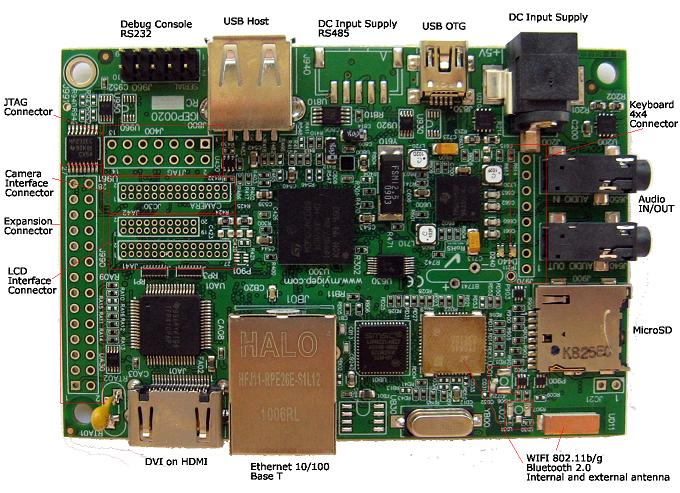
This wiki has information about IGEP connectors.
More information in schematics.
Connectors
IGEPv2

|
Table information:
- Pad number. See PCB.
- "Connect to" is a name used in schematics, usually it will be default peripheral name (mode=0)
- IGEP main peripheral
- Main utility
- Other available peripherals. See this page for more information
- "Share with" is alternate configuration for pad. See this page for more information
J990 connector
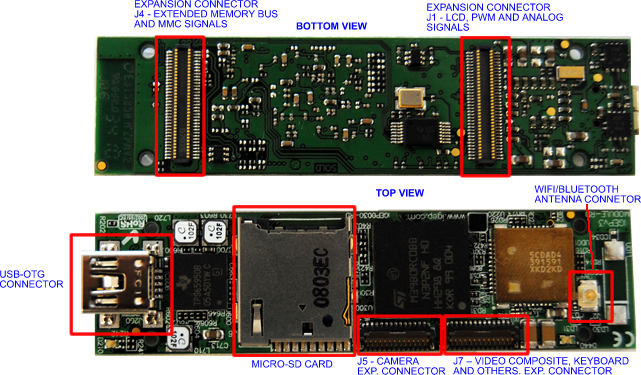
This connector is used mainly to add new features to IGEPv2 using a Expansion. WIFI/BT combo is not avalaible in some versions.
| Pad | Connect to |
Main peripheral |
Main utility |
Other available peripherals | Share with |
| 1 | VIO 1V8 | - | Power 1v8 | - | - |
| 2 | DC 5V | - | Power 5v | - | - |
| 3 | MMC2_DAT7 |
GPIO_139(mode=4) |
Reset WIFI |
MMC2_DAT7(mode=0) MMC2_CLKIN(mode=1) MMC3_DAT3(mode=3) |
WIFI/BT combo:WIFI |
| 5 | MMC2_DAT6 |
GPIO_138(mode=4) |
Power down WIFI |
MMC2_DAT6(mode=0) MMC2_DIR_CMD(mode=1) MMC3_DAT2(mode=3) |
WIFI/BT combo:WIFI |
| 7 | MMC2_DAT5 |
GPIO_137(mode=4) |
Reset BT |
MMC2_DAT5(mode=0) MMC2_DIR_DAT1(mode=1) MMC3_DAT1(mode=3) |
WIFI/BT combo:BT |
| 9 | MMC2_DAT4 |
GPIO136(mode=4) |
- |
MMC2_DAT4(mode=0) MMC_DIR_DAT0(mode=1) MMC3_DAT0(mode=3) |
WIFI/BT combo:WIFI |
| 11 | MMC2_DAT3 | MMC2_DAT3(mode=0) | Transfer data |
McSPI3_CS0(mode=1) GPIO_135(mode=4) |
WIFI/BT combo:WIFI |
| 13 | MMC2_DAT2 | MMC2_DAT2(mode=0) | Transfer data |
McSPI3_CS1(mode=1) GPIO_134(mode=4) |
WIFI/BT combo:WIFI |
| 15 | MMC2_DAT1 | MMC2_DAT1(mode=0) | Transfer data between Omap and WIFI | GPIO_133(mode=4) | WIFI/BT combo:WIFI |
| 17 | MMC2_DAT0 | MMC2_DAT0(mode=0) | Transfer data |
McSPI3_SOMI(mode=1) GPIO_132(mode=4) |
WIFI/BT combo:WIFI |
| 19 | MMC2_CMD | MMC2_CMD(mode=0) | Control Wire for bus MMC2 (WIFI) |
McSPI3_SIMO(mode=1) GPIO_131(mode=4) |
WIFI/BT combo:WIFI |
| 21 | MMC2_CLK0 | MMC2_CLK(mode=0) | Clock for MMC2 (WIFI) |
McSPI3_CLK(mode=1) GPIO_130(mode=4) |
WIFI/BT combo:WIFI |
| 4 | MCBSP3_DX | MCBSP3_DX (mode=0) | Transmitted serial Data (BT audio) |
UART2_CTS(mode=1) GPIO_140(mode=4) |
TPS65950: PCM VSP |
| 6 | MCBSP3_CLKX | MCBSP3_CLKX(mode=0) | Transmitted serial Clock (BT audio) |
UART2_TX(mode=1) GPIO_142(mode=4) |
BT/TPS65950: PCM VSP |
| 8 | MCBSP3_FSX | MCBSP3_FSX (mode=0) | Transmited Frame Syncronisation (BT audio) |
UART2_RX(mode=1) GPIO_143(mode=4) |
BT/TPS65950: PCM VSP |
| 10 | MCBSP3_DR | MCBSP3_DR (mode=0) | Received Serial Data (BT audio) |
UART2_RTS(mode=1) GPIO_141(mode=4) |
TPS65950: PCM VSP |
| 12 | MCBSP1_DX |
GPIO_158(mode=4) |
- |
MCBSP1_DX McSPI4_SIMO(mode=1) McBSP3_DX(mode=2) |
- |
| 14 | MCBSP1_CLKX |
GPIO_162(mode=4) |
- |
MCBSP1_CLKX McBSP3_CLKX(mode=2) |
- |
| 16 | MCBSP1_FSX |
GPIO_161(mode=4) |
- |
MCBSP1_FSX McSPI4_CS0(mode=1) McBSP3_FSX(mode=2) |
- |
| 18 | MCBSP1_DR |
GPIO_161(mode=4) |
- |
MCBSP1_DR McSPI4_SOMI(mode=1) McBSP3_DR(mode=2) |
- |
| 20 | MCBSP1_CLKR |
GPIO_156(mode=4) |
- |
MCBSP1_CLKR |
- |
| 22 | MCBSP1_FSR |
GPIO_157(mode=4) |
- |
MCBSP1_FSR |
- |
| 23 | I2C2_SDA | I2C2_SDA(mode=0) | I2C Data |
GPIO_183(mode=4) |
CAM if configured via hardware: RC14 |
| 24 | I2C2_SCL | I2C2_SCL(mode=0) | I2C Clock |
GPIO_168(mode=4) |
CAM if configured via hardware: RC13 |
| 25 | REGEN | - | Master/Slave control power TPS65950 | - | - |
| 26 | nRESET | - | Read Reset Omap | - | - |
| 27 | GND | - | GND | - | - |
| 28 | GND | - | GND | - | - |
J960 connector
This connector is used mainly to connect via serie to IGEP Software using RS232 standard. See Schematics for more information.
| Pad | Connect to | Main peripheral | Main utility | Other available peripherals (only via hardware) |
Share with |
| 1 | - | - | - |
- | - |
| 2 | RS232_RX2 | UART3_RX(R966) | Serial debug |
UART2_RX(R952) | SN65C3232EPW |
| 3 | RS232_TX2 | UART3_TX(R965) | Serial debug |
UART2_TX(R947) | SN65C3232EPW |
| 4 | - | - | - |
- | - |
| 5 | GND | - | GND | - | - |
| 6 | GND | - | GND | - | - |
| 7 | - | - | - |
- | - |
| 8 | RS232_TX1 | UART1_TX(R961) | SN65C3232EPW | UART3_TX(R940) | SN65C3232EPW |
| 9 | RS232_RX1 | UART1_RX(R962) | SN65C3232EPW | UART3_RX(R942) | SN65C3232EPW |
| 10 | - | - | - |
- | - |
J940 connector
This connector is used mainly to connect via RS485 (UART1) with other devices
| Pad | Connect to | Main peripheral | Main utility | Other available peripherals |
Share with |
| 1 | PWR_GND | GND | - |
- | - |
| 2 | PWR_5V | Power 5v |
- |
- | - |
| 3 | PWR_9V | Power 9v |
- |
- | - |
| 4 | RS485_A | UART3_RX/UART3_TX | A aka '−' aka TxD-/RxD- aka inverting pin | - | TXS0102DCUR |
| 5 | RS485_B | UART3_RX/UART3_TX | B aka '+' aka TxD+/RxD+ aka non-inverting pin | - | TXS0102DCUR |
J400 connector
J400 is used to JTAG (Joint Test Action Group). JTAG is a standardized serial protocol widely used in printed circuit boards. Its main functions are:
-Debug the software of an embedded system directly
-Storing firmware
-Boundary scan testing
| Pad | Connect to | Main peripheral | Main utility | Other available peripherals |
Share with |
| 1 | JTAG_TMS | JTAG_TMS |
|
- | - |
| 2 | JTAG_NTRST | JTAG_NTRST |
|
- | - |
| 3 | JTAG_TDI | JTAG_TDI |
|
- | - |
| 4 | GND | - | GND | - | - |
| 5 | 1V8 | Power 1V8 |
|
- | - |
| 6 | - | - | |
- | - |
| 7 | JTAG_TD0 | JTAG_TD0 |
|
- | - |
| 8 | GND | - | GND | - | - |
| 9 | JTAG_RTCK | JTAG_RTCK |
|
- | - |
| 10 | GND | - | GND | - | - |
| 11 | JTAG_TCK | JTAG_TCK |
|
- | - |
| 12 | GND | - | GND | - | - |
| 13 | JTAG_EMU0 | JTAG_EMU0(mode=0) |
|
GPIO_11(mode=4) | - |
| 14 | JTAG_EMU1 | JTAG_EMU1(mode=0) |
|
GPIO_31(mode=4) | - |
J970 connector
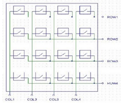
J970 is used to implement a keypad. It is controlled by TPS65950, this method avoid reduce Omap proces capabilities. TPS65950 send via I2C1 all the interrupt request. Their characteristics are:
- Can handle up to 8 x 8 keypads, IGEPv2 can handle up to 4 x 4 keypads.
- Optionally, you can decode via Omap software.
- Event detection on key press and key release.
- Multikey press detection, can detect up 2 keys at the same time.
- Long-key detection on prolonged key press.
- Programmable time-out on permanent key press or after keypad release.
The next table show J970 connector information:
| Pad | Connect to: |
| 1 | KPD_C0 |
| 2 | KPD_C1 |
| 3 | KPD_C2 |
| 4 | KPD_C3 |
| 5 | KPD_R0 |
| 6 | KPD_R1 |
| 7 | KPD_R2 |
| 8 | kPD_R3 |

|
More information in TPS65950 datasheets.
JC30 connector
JC30 is used to connect a camera for capture video or image. Omap have the processing capability to connect RAW image-sensor modules via this connector. But default kernel 2.6.35.y cam is not enable.
The next table show JC30 connector information:
| Pad: | Connect to: | Default peripheral | Other peripheral: (via Hardware) |
| 1 | CAM_HS | GPIO_94 | - |
| 2 | CAM_VS | GPIO_95 | - |
| 3 | CAM_XCLKA | GPIO_96 | - |
| 4 | GND | - | - |
| 5 | CAM_PCLK | GPIO_97 | - |
| 6 | GND | - | - |
| 7 | CAM_DO | GPIO_99 | - |
| 8 | CAM_FLD | GPIO_98 | - |
| 9 | CAM_D2 | GPIO_101 | - |
| 10 | CAM_D1 | GPIO_100 | - |
| 11 | CAM_D4 | GPIO_103 | - |
| 12 | CAM_D3 | GPIO_102 | - |
| 13 | CAM_D6 | GPIO_105 | - |
| 14 | CAM_D5 | GPIO_104 | - |
| 15 | CAM_D8 | GPIO_107 | - |
| 16 | CAM_D7 | GPIO_106 | - |
| 17 | CAM_D10 | GPIO_109 | - |
| 18 | CAM_D9 | GPIO_108 | - |
| 19 | CAM_XCLKB | GPIO_111 | - |
| 20 | CAM_D11 | GPIO_110 | - |
| 21 | GPIO_112/I2C2_SCL |
GPIO_112 (RC11) |
I2C2_SCL: RC13 |
| 22 | GPIO_113/I2C2_SDA |
GPIO_113 (RC12) |
I2C2_SDA: RC14 |
| 23 | CAM_RESET | GPIO_114 | - |
| 24 | CAM_PDN | GPIO_115 | - |
| 25 | CAM_STROBE | GPIO_126 | - |
| 26 | CAM_WEN | GPIO_167 | - |
| 27 | 3V3 | - | - |
| 28 | 3V3 | - | - |
JA42 connector
JA42 is used for DVI (Digital Video Interface) control part, TouchScreen control and SPI1.
The next table show JA42 connector information:
| Pad: | Connect to: |
Default peripheral (mode=0) |
Default function: | Other available peripherals: | Share with: |
| 1 | VIO 1V8 | - | Power 1v8 | - | - |
| 2 | SYS_BOOT5 |
SYS_BOOT5 |
Omap boot config |
MMC2_DIR_DAT(mode=1) GPIO_7 (mode=4) |
- |
| 3 | DC_5V | - | Power 5v | - | - |
| 4 | GND | - | GND | - | - |
| 5 | SYS_BOOT0 |
SYS_BOOT0 |
Omap boot config |
GPIO_2 (mode=4) |
- |
| 6 | SYS_BOOT1 |
SYS_BOOT1 |
Omap boot config |
GPIO_3 (mode=4) |
- |
| 7 | DVI_VSYNC | DSS_VSYNC | LCD vertical sync (Expansion) |
GPIO_68(mode=4) |
TFP410 |
| 8 | DVI_HSYNC | DSS_HSYNC | LCD Horitzontal sync (Expansion) |
GPIO_67 (mode=4) |
TFP410 |
| 9 | DVI_ACBIAS | DSS_ACBIAS | LCD Control (Expansion) | GPIO_133(mode=4) | TFP410 |
| 10 | DVI_PUP | - | Control signal for DVI controler (Expansion) | - | TFP410 |
| 11 | DVI_PCLK | DSS_PCLK | LCD clock (Expansion) |
GPIO_66 (mode=4) |
TFP410 |
| 12 | TS_nPEN_IRQ | McSPI1_CS1 | Touchscreen control (Expansion) |
GPIO_175 (mode=4) |
- |
| 13 | LCD_QVGA/nVGA | McBSP4_DX | Touchscreen control (Expansion) |
GPIO_154 (mode=4) |
- |
| 14 | LCD_ENVDD | McBSP4_DR | Touchscreen control (Expansion) |
GPIO_153 (mode=4) |
- |
| 15 | LCD_RESB | McBSP4_FSX | Touchscreen control (Expansion) |
GPIO_155 (mode=4) |
- |
| 16 | LCD_INI | McBSP4_CLKX | Touchscreen control (Expansion) |
GPIO_152 (mode=4) |
- |
| 17 | MCSPI1_CLK |
McSPI1_CLK |
Touchscreen control (Expansion) |
GPIO_171 (mode=4) |
- |
| 18 | MCSPI1_SIMO | McSPI1_SIMO | Touchscreen control (Expansion) |
GPIO_172 (mode=4) |
- |
| 19 | MCSPI1_CS0 | McSPI1_CS0 | Touchscreen control (Expansion) |
GPIO_174 (mode=4) |
- |
| 20 | MCSPI1_SOMI | McSPI1_SOMI | Touchscreen control (Expansion) |
GPIO_173 (mode=4) |
- |
TFP410: converts DVI signal to HDMI
JA41 connector
JA41 is used for DVI (Digital Video Interface) data part.
The next table show JA41 connector information:
| Pad: | Connect to: |
Default peripheral (mode=0) |
Default function: | Other available peripherals: | Share with: |
| 1 | VIO 3V3 | - | Power 3v3 | - | - |
| 2 | GND |
- |
GND |
- |
- |
| 3 | DVI_DATA0 | DSS_D0 | LCD pixel data bit |
UART1_CTS(mode=2) GPIO_70(mode=4) |
TFP410 |
| 4 | DVI_DATA1 | DSS_D1 | LCD pixel data bit |
UART1_RTS(mode=2) GPIO_71(mode=4) |
TFP410 |
| 5 | DVI_DATA2 |
DSS_D2 |
LCD pixel data bit |
GPIO_72(mode=4) |
TFP410 |
| 6 | DVI_DATA3 |
DSS_D3 |
LCD pixel data bit |
GPIO_73(mode=4) |
TFP410 |
| 7 | DVI_DATA4 | DSS_D4 | LCD pixel data bit |
UART3_RX(mode=2) GPIO_74(mode=4) |
TFP410 |
| 8 | DVI_DATA5 | DSS_D5 | LCD pixel data bit |
UART3_TX(mode=2) GPIO_75(mode=4) |
TFP410 |
| 9 | DVI_DATA6 | DSS_D6 | LCD pixel data bit |
UART1_TX(mode=2) GPIO_76(mode=4) |
TFP410 |
| 10 | DVI_DATA7 | DSS_D7 | LCD pixel data bit |
UART1_RX(mode=2) GPIO_77(mode=4) |
TFP410 |
| 11 | DVI_DATA8 | DSS_D8 | LCD pixel data bit |
GPIO_78(mode=4) |
TFP410 |
| 12 | DVI_DATA9 | DSS_D9 | LCD pixel data bit |
GPIO_79(mode=4) |
TFP410 |
| 13 | DVI_DATA10 | DSS_D10 | LCD pixel data bit |
GPIO_80(mode=4) |
TFP410 |
| 14 | DVI_DATA11 | DSS_D11 | LCD pixel data bit |
GPIO_81(mode=4) |
TFP410 |
| 15 | DVI_DATA12 | DSS_D12 | LCD pixel data bit |
GPIO_82(mode=4) |
TFP410 |
| 16 | DVI_DATA13 | DSS_D13 | LCD pixel data bit |
GPIO_83(mode=4) |
TFP410 |
| 17 | DVI_DATA14 |
DSS_D14 |
LCD pixel data bit |
GPIO_84(mode=4) |
TFP410 |
| 18 | DVI_DATA15 | DSS_D15 | LCD pixel data bit |
GPIO_85(mode=4) |
TFP410 |
| 19 | DVI_DATA16 | DSS_D16 | LCD pixel data bit |
GPIO_86(mode=4) |
TFP410 |
| 20 | DVI_DATA17 | DSS_D17 | LCD pixel data bit |
GPIO_87(mode=4) |
TFP410 |
| 21 | DVI_DATA18 | DSS_D18 | LCD pixel data bit |
DSS_D0 (mode=3) MCSPI3_CLK(mode=2) GPIO_88(mode=4) |
TFP410 |
| 22 | DVI_DATA19 | DSS_D19 | LCD pixel data bit |
DSS_1 (mode=3) MCSPI3_SIMO(mode=2) GPIO_89(mode=4) |
TFP410 |
| 23 | DVI_DATA20 | DSS_D20 | LCD pixel data bit |
DSS_D2 (mode=3) MCSPI3_SOMI(mode=2) GPIO_90(mode=4) |
TFP410 |
| 24 | DVI_DATA21 | DSS_D21 | LCD pixel data bit |
DSS_3 (mode=3) MCSPI3_CSO(mode=2) GPIO_91(mode=4) |
TFP410 |
| 25 | DVI_DATA22 | DSS_D22 | LCD pixel data bit |
DSS_D4 (mode=3) MCSPI3_CS1(mode=2) GPIO_92(mode=4) |
TFP410 |
| 26 | DVI_DATA23 | DSS_D23 | LCD pixel data bit |
DSS_D5(mode=3) GPIO_93(mode=4) |
TFP410 |
| 27 | I2C3_SCL | I2C3_SCL | I2C3 interface |
GPIO_184(mode=4) |
TXS0102DCUR |
| 28 | I2C3_SDA | I2C3_SDA | I2C3 interface |
GPIO_185(mode=4) |
TXS0102DCUR |
TFP410: converts DVI signal to HDMI
TXS0102DCUR: Increse I2c3 voltage to 5V to read EDID information
IGEP MODULE

|
Under construction


