Mux configuration
From IGEP - ISEE Wiki
Contents
Overview
This How-To is meant to be a starting point for people to learn configure mux for IGEP v2 devices as quickly and easily as possible. For this how-to i used Linaro Headless and Ubuntu 10.04 with Linaro Toolchain.
Mux (or multiplexer) is a Omap peripheral that can be controlled via software. Its function is connect other peripherals to some available Omap pins.
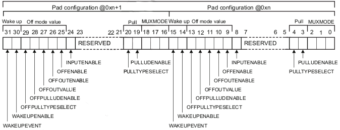
Each pin is configurable by software using its associated pad configuration register field, which is 16 bits wide:

|
One pad configuration register field is available for each pin. Each 32-bit pad configuration register is grouped into two 16-bit pad configuration register fields. One pad configuration register provides control for two different pins. These registers can be accessed using 8, 16 and 32 bits operations.
The functional bits of a pad configuration register field are divided into the following five fields:
• MUXMODE (3 bits) defines the multiplexing mode applied to the pin. A mode corresponds to the selection of the functionality mapped on the pin with six (0 to 5) possible functional modes for each pin.
• PULL (2 bits) for combinational pullup/pulldown configuration:
-> PULLTYPESELECT: Pullup/pulldown selection for the pin.
-> PULLUDENABLE: Pullup/pulldown enable for the pin.
• INPUTENABLE (1 bit) drives an input enable signal to the I/O CTRL.
• Off mode values (5 bits) override the pin state when the OFFENABLE bit CONTROL. This feature is used for power saving management:
->OFFENABLE: Off mode pin state override control. Set to 1 to enable the feature and to 0 to disable it.
->OFFOUTENABLE: Off mode output enable value. Set to 0 to enable the feature and to 1 to disable it.
->OFFOUTVALUE: Off mode output value.
->OFFPULLUDENABLE: Off mode pullup/pulldown enable.
->OFFPULLTYPESELECT: Off mode pullup/pulldown selection.
• Wake-up bits (2 bits):
->WAKEUPENABLE: Enable wake-up detection on input. It is also the off mode input enable value.
->WAKEUPEVENT: Wake-up event status for the pin.
NOTE: Off mode can be configured like pin output with a HIGH or LOW value or pin input with wake-up detection feature.
NOTE: For input pins, OFFOUTENABLE and OFFOUTVALUE bits can not be configured.
|
|
Mode selection
| MUXMODE | Select Mode |
| 0b000=0 | Mode 0 (Primary mode) |
| 0b001=1 | Mode 1 (Possible mode) |
| 0b010=2 | Mode 2 (Possible mode) |
| 0b011=3 | Mode 3 (Possible mode) |
| 0b100=4 | Mode 4 (Possible mode) |
| 0b101=5 | Mode 5 (Possible mode) |
| 0b110=6 | Mode 6 (Possible mode) |
| 0b111=7 | Mode 7 (Safe Mode) |
Mode 0 is the primary mode. When mode 0 is set, the function mapped to the pin corresponds to the name of the pin.
Mode 1 to mode 6 are possible modes for alternate functions. On each pin, some modes are used effectively for alternate functions, while other modes are unused and correspond to no functional configuration.
The safe mode (default mode 7) avoids any risk of electrical contention by configuring the pin as an input with no functional interface mapped to it. The safe mode is used mainly as the default mode for all pins containing no mandatory interface at the release of power-on reset.
NOTE: For most pads, the reset value for the MUXMODE field is 0b111. The exceptions are pads to be used at boot time to transfer data from selected peripherals to the external flash memory.
Pull Selection
Note: when a pin is in output mode, pulls are automatically disable.
| PULLTYPESELECT | PULLUDENABLE | Pin Behavior |
| 0b0 | 0b0 | Pull-down selected but not activated |
| 0b0 | 0b1 | Pull-down selected and activated if pin is NOT configured as OUTPUT |
| 0b1 | 0b0 | Pull-up selected but not activated |
| 0b1 | 0b1 | Pull-up selected and activated if pin is NOT configured as OUTPUT |
Input Enable
INPUTENABLE = 0: Input Disable. Pin is configured in output only mode.
INPUTENABLE = 1: Input Enable. Pin is configured in bidirectional mode.
NOTE: For proper functioning of some peripherals INPUTENABLE must be set to 1 for pads configured to drive output clocks:
- SDRC
- GPMC
- McSPIi
- I2Ci
- MMCi
- McBSPi
- HSUSB HOST
Off mode values and Wake-up
This mode is used to disable some pins and reduce low power consumption.
Please contribute ..
IGEP
Important tips
Use the following tips to configure mux without problems:
- Mux can connect multiple connectors at the same peripheral, this improper use can damage the processor. Make sure to disable old connector configuration before use new one.
- Some peripherals are only available if you place or replace some resistances. View schematics for more information.
- Some connectors share multiples peripherals. You should disable unused peripherals to avoid interferences. For example: if you want to control WIFI module via J990 disable OMAP or if you want use UART2 at j990 disable Bluetooth.
Configure mux
IgepV2 Board have a default mux configuration, but some cases is necessary change it, for example your project need UART2 at j990 connector to transmit data, for this purpose you need change some mux configurations to enable it and be sure that this modification don't break or interferes in other IC or peripherals. The mux options are vast. There are three ways to configure mux at DM37xx and OMAP35xx:
- Editing OS User Space. this mode has a issue, when your system reboot or shutdown you will need to configure again. Example.
- Using kernel buddies. This way is ot avaliable in some cases. Example.
- Editing and compile kernel sources. Example.
More information about mux.
Feedback and Contributing
At any point, if you see a mistake you can contribute to this How-To.
Available peripherals on external connector
The next tables show you all the mux capabilities:
| J990 | J960 | J970 | J400 | |
| UART1 | No | Yes | No | No |
| UART2 | Yes | Yes, via hardware | No | No |
| UART3 | No | Yes (default) | No | No |
| UART4 | No | No | No | No |
| GPIO | Yes | No | No | Yes |
| McSPI1 | Yes (default) | No | No | |
| McSPI2 | No | No | ||
| McSPI3 | No | No | ||
| McSPI4 | No | No | ||
| McBSP1 | No | No | ||
| McBSP2 | No | No | ||
| McBSP3 | No | No | ||
| McBSP4 | No | No | ||
| McBSP5 | No | No | ||
| MMC1 | No | No | ||
| MMC2 | No | No | ||
| MMC3 | No | No | ||
| I2C1 | No | No | ||
| I2C2 | No | No | ||
| I2C3 | No | No | ||
| I2C4 | No | No |
| JC30 | JA42 | JA41 | TP | |
| UART1 | No | No | No | No |
| UART2 | No | No | No | No |
| UART3 | No | No | No | No |
| UART4 | No | No | No | No |
| GPIO | Yes | Yes | Yes | Yes |
| McSPI1 | ||||
| McSPI2 | ||||
| McSPI3 | ||||
| McSPI4 | ||||
| McBSP1 | ||||
| McBSP2 | ||||
| McBSP3 | ||||
| McBSP4 | ||||
| McBSP5 | ||||
| MMC1 | ||||
| MMC2 | ||||
| MMC3 | ||||
| I2C1 | ||||
| I2C2 | ||||
| I2C3 | ||||
| I2C4 |
Under construction


