Difference between revisions of "IMX6 Quad"
From IGEP - ISEE Wiki
(→Documentation) |
|||
| Line 49: | Line 49: | ||
* [https://www.nxp.com/docs/en/fact-sheet/IMX6SRSFS.pdf i.MX 6 Series of Applications Processors Fact Sheet] | * [https://www.nxp.com/docs/en/fact-sheet/IMX6SRSFS.pdf i.MX 6 Series of Applications Processors Fact Sheet] | ||
* [https://www.nxp.com/docs/en/reference-manual/IMX6DQRM.pdf i.MX 6Dual/6Quad Applications Processor Reference Manual] | * [https://www.nxp.com/docs/en/reference-manual/IMX6DQRM.pdf i.MX 6Dual/6Quad Applications Processor Reference Manual] | ||
| − | |||
==See also== | ==See also== | ||
Revision as of 11:09, 4 April 2018
NXP i.MX6 Quad
CPU Complex
- 4x ARM Cortex-A9 up to 1.2 GHz
- NEON SIMD media accelerator
Memory
DDR
- 2x32 LP-DDR2, 1x64 DDR3 / LV-DDR3
NAND
- SLC/MLC, 40-bit ECC, ONFI2.2, DDR
Connectivity
- S-ATA and PHY
Advanced power management
PMU integration
NXP PF100 power management unit
Package and temperature
- 21 x 21mm, 0.8 mm BGA
- Consumer (-20C to +105C), up to 1.2 GHz
- Industrial (-40C to +105C), up to 800 MHz
- Automotive (-40C to +125C), AEC-Q100, up to 1 GHz
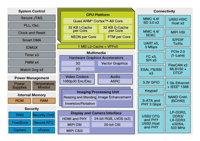
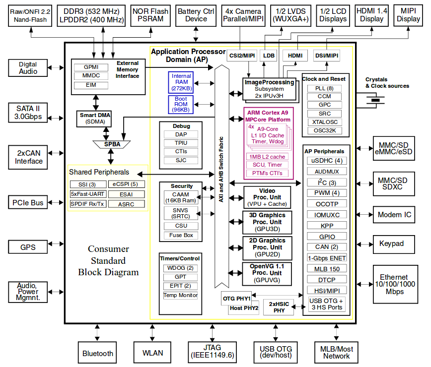
Block diagram
Documentation
- i.MX 6Dual/6Quad Applications Processors for Consumer Products - Data Sheet
- i.MX 6Dual/6Quad Automotive and Infotainment Applications Processors - Data Sheet
- i.MX 6Dual/6Quad Consumer-PoP Applications Processor Data Sheet
- i.MX 6Dual/6Quad Applications Processors for Industrial Products - Data Sheet
- IMX6DQ6SDLHDG, Hardware Development Guide for i.MX 6Quad, 6Dual, 6DualLite, 6Solo Families of Applications Processors
- i.MX 6 Series of Applications Processors Fact Sheet
- i.MX 6Dual/6Quad Applications Processor Reference Manual


